Electrode structure of LED and manufacturing of the same

a technology of light emitted diodes and electrodes, which is applied in the direction of basic electric elements, electrical equipment, semiconductor devices, etc., can solve the problems of short life time of leds, lattice defects, and junction damage, and achieve the effect of improving light emitted efficiency

Inactive Publication Date: 2003-08-07
HEN CHANG HSIU
View PDF0 Cites 79 Cited by
  • Summary
  • Abstract
  • Description
  • Claims
  • Application Information

AI Technical Summary

Benefits of technology

0010] Another object of the present invention is to provide an electrode structure of light emitted diode with reflective metal around the chip to enhance the light emitting efficiency by reflecting the light emitted from the pn-junction to the reflective layer under the chip, and reflecting upward again. This makes the light emitted e

Problems solved by technology

The electrode of a conventional LED on the center makes the electric field spreading uniformly around the chip, but gold and aluminum is opaqueness, light is blocking by the electrode too much if the electrode is large, but if too small, electric field would crowded in the center and the current density is increasing, this causes short life time of the LED, also in the center there will be a d

Method used


Image

  • Electrode structure of LED and manufacturing of the same
  • Electrode structure of LED and manufacturing of the same
  • Electrode structure of LED and manufacturing of the same

Examples


first embodiment

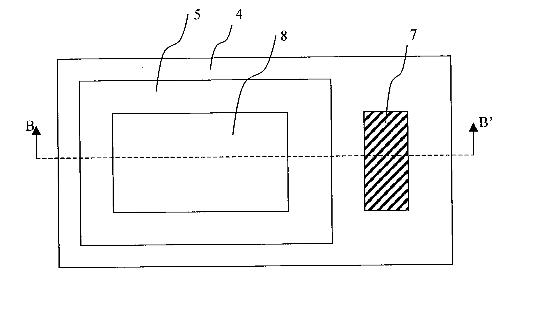
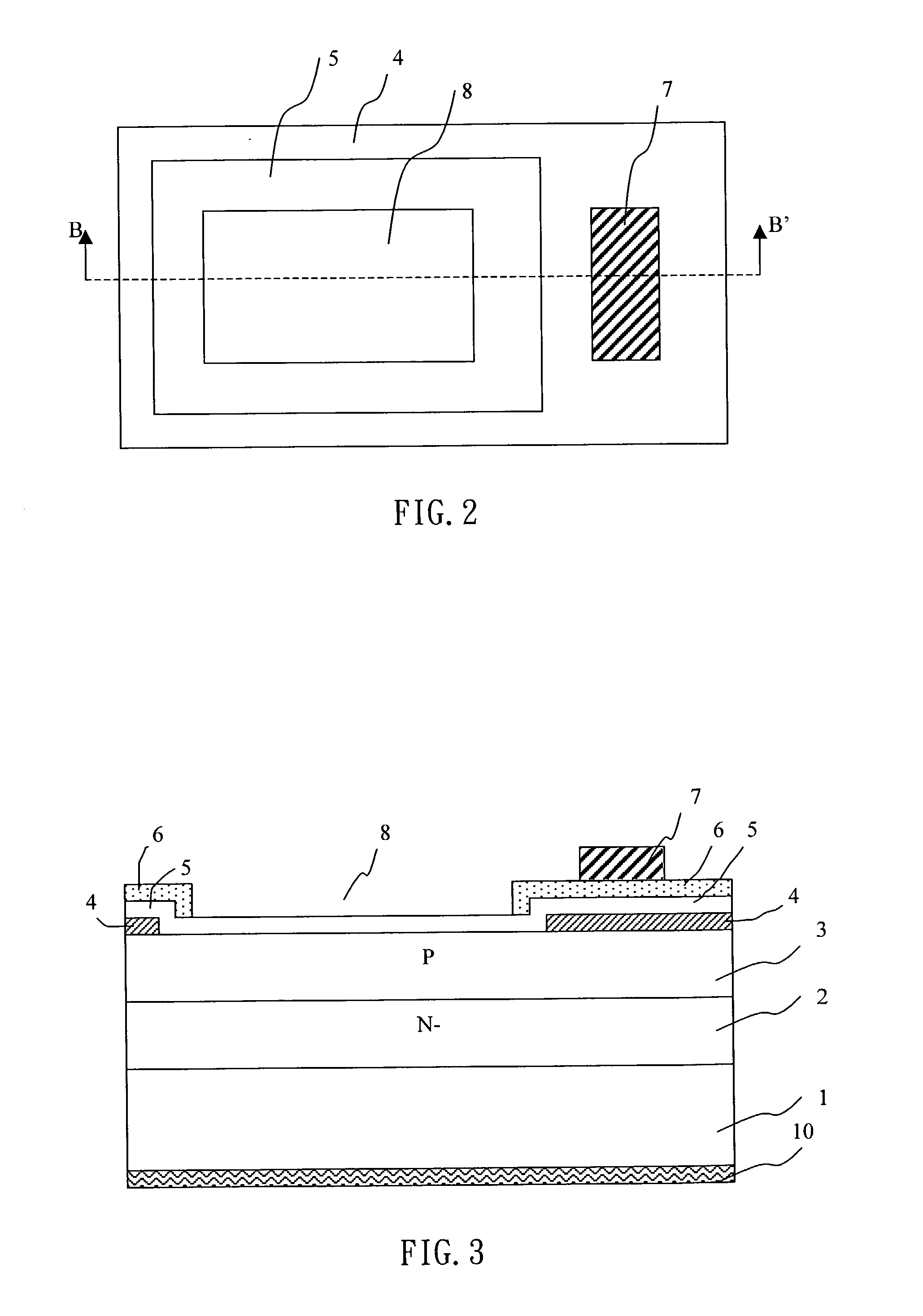
[0024] FIG. 2 shows the electrode structure of a bottom layer LED for overlap cascaded packaging of the present invention. FIG. 3 is the cross section along BB' of FIG. 2. Substrate 1 is always a non transparent .quadrature.-.quadrature.group or .quadrature.-.quadrature. group compound semiconductor such as GaAs,GaP or GaN. A layer of n-type semiconductor 2 is formed by epitaxy technology on the substrate 1(see the cross sectional view of FIG. 3). Then a p-type semiconductor 3 is expitaxied to form a pn- junction as the light emitted diode. The pn- junction may be double hetero structure or quantum well structure. An electrode structure of the present invention is formed on the p-type semiconductor: First, a silicon dioxide layer 4 of 1000 .ANG. to 10000 .ANG. is deposited on the p-type semiconductor. By using a first mask in lithography and etching process to etch away the silicon dioxide to form an open window and keep the silicon dioxide around the chip and under the bonding pad ...

second embodiment

[0029] FIG. 8A, 8b, 8C and 8D are the manufacturing steps of the electrodes of a LED according to the present invention. As shown in FIG. 8A, n-type semiconductor 2 and p-type semiconductor 3 are epitaxied on a sapphire substrate 1, then etch away a strip of p-type semiconductor by lithography and etching to form a step 14 with width of 100-200 .mu.m, the n-type semiconductor 2 under the step 14 is then exposed. As in FIG. 8B, a silicon dioxide of thickness 1000 .ANG. to 1000 .ANG. is deposited, a first mask is used to pattern the silicon dioxide, remove the oxide on the contact area and keep the oxide 4 around the periphery of the chip and under the positive bonding pad 7. The width of the oxide 4 is 5-20 .mu.m except that under the positive bonding pad. Under the positive bonding pad 7 the oxide 4 is wider than the positive bonding pad 7 for absorbing the stress of wire bonding. Under the negative bonding pad, the oxide 4 is removed except around the periphery of the chip and arou...


PUM


Abstract

The present invention discloses an electrode structure of a light emitted diode and manufacturing method of the electrodes. After formed a pn-junction 2, 3 of a light emitted diode on a substrate 1, a layer of SiO2 is deposited on the periphery of the LED die near the scribe line of the wafer, then a transparent conductive layer 5 is deposited, then a layer of gold or AuGe etc 6, is formed with an opening on the center of the die. After forming alloy with the semiconductor by heat treatment to form ohmic contact, a strip of aluminum (Al) 7 is formed on one side of the die on the front side for wire bonding and to be the positive electrode of the LED. The negative electrode 10 is formed on the substrate by metal contact. Another form of the electrode structure of the present invention is making both the positive electrode 7 and negative electrode 7a on the front side of the LED by etching the p-type semiconductor 3 of the pn-junction and forming a strip of negative electrode 7a on the n-type semiconductor area 2, the positive electrode is formed on the p-type semiconductor area.

Description

[0001] 1. Field of the Invention[0002] The present invention relates to an electrode structure of semiconductor light emitted diodes (LED) and manufacturing method, and more particularly, to an electrode structure of LED suitable for overlap cascaded packaging.[0003] 2. Description of Relative Prior Art[0004] Light emitted diode (LED) is a semiconductor light-emitting device, formed by a pn-junction, to transform electric power into a light source. LED has characteristics such as small volume, long life-time, low driving voltage, shock hardness, thermal stability, etc., suitable for applications which need to be thin and small, and used in traffic signals, back light source of LCD and other commercial products.[0005] LED make use of variety of compound semiconductor such as .quadrature.-.quadrature.group materials,.quadrature.-VI group materials, to form variety structures such as pn junction, double-hetero-junction(DH-) and quantum well(QW), which can be used to design red, orange,...

Claims


Application Information

Patent Timeline
IPC IPC(8): H01L33/38H01L33/40
CPCH01L33/405H01L33/38
Inventor HEN, CHANG HSIU
Owner HEN CHANG HSIU
Why Eureka
Try Eureka