Semiconductor device and method of manufacturing the semiconductor device

a semiconductor and semiconductor technology, applied in the direction of semiconductor devices, semiconductor/solid-state device details, electrical apparatus, etc., can solve the problems of not so effective, much lower dielectric constant, and reduced dielectric constant of semiconductor devices, so as to reduce the effective relative dielectric constant of interlayer insulating films, reduce the delay in signal propagation through wirings, and simplify the process steps

Inactive Publication Date: 2003-10-16
RENESAS ELECTRONICS CORP
View PDF4 Cites 75 Cited by
  • Summary
  • Abstract
  • Description
  • Claims
  • Application Information

AI Technical Summary

Benefits of technology

0011] On the basis of the aforementioned technical background, the present invention proposes to solve the above-mentioned problems by using an organic insulating film in an interlayer insulating film and to simplify the process steps at the same time. Effective relative

Problems solved by technology

Consequently, the time of delay in propagation of signals through wirings, i.e. delay in signal propagation through wirings, becomes longer, causing a serious problem in the use of semiconductor device-mounted electronic appliances.
However, owing to the still relatively high dielectric constant, the SiO.sub.2 film is not so effective for lowering the interlayer capacitance, when used as an interlayer insulating film, and thus materials of much lower dielectric constant are required for the next or further

Method used


Image

  • Semiconductor device and method of manufacturing the semiconductor device
  • Semiconductor device and method of manufacturing the semiconductor device
  • Semiconductor device and method of manufacturing the semiconductor device

Examples


example 1

[0083] FIG. 2 shows process steps of producing a semiconductor device according to a first embodiment of the present invention.

[0084] At first, an organic insulating film material FLARE.TM. (a trade name, polyarylene ether, 7

[0085] wherein AR.sup.0, AR.sup.1 are aromatic groups, made by Honeywell, Ltd.) is spin coated onto semiconductor substrate 201 of silicon or the like by a well known spinner and heated on a hot plate successively at temperatures such as 150.degree., 200.degree. C. and 250.degree. C. each for one minute to form first insulating layer 202 in a semi-thermosetting state [FIG. 2(a)], where first insulating layer 202 is 400 nm thick.

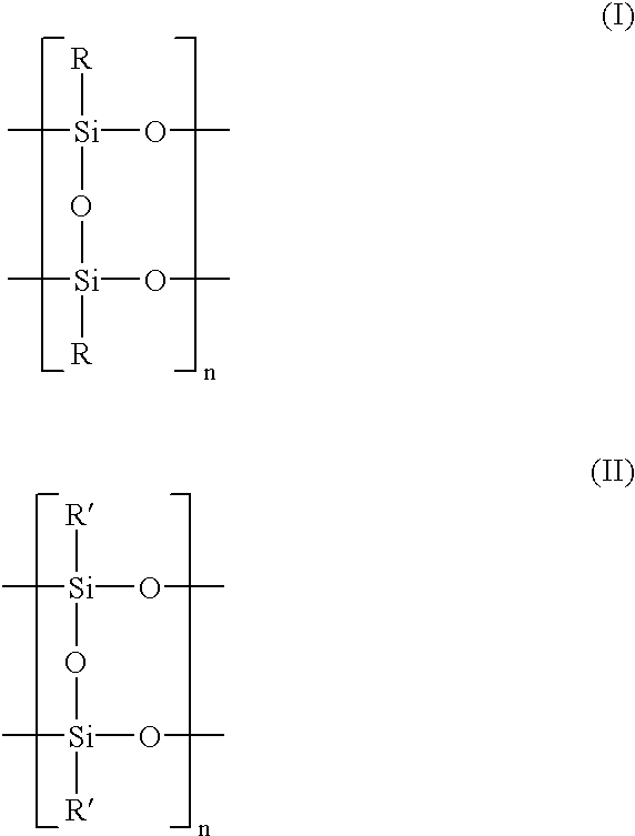
[0086] Then, ladder silicone-based polymer material represented by the following formula (III) [number average molecular weight (Mn)=2,032; weight average molecular weight (Mw)=2,576, .gamma. (Mw / Mn)=1.27 (where molecular weights are determined by liquid chromatography based on ultraviolet ray absorption as a detector)] is spin coated ont...

example 2

[0096] FIG. 3 shows process steps of producing a semiconductor device according to a second embodiment of the present invention.

[0097] Process step of forming first insulating layer 302 (film thickness: 400 nm) in a semi-thermosetting state, from an organic insulating film material FLARE.TM. (trademark of a product made by Honeywell, Ltd.) on semiconductor substrate 301 of silicon or the like is the same as in Example 1 [FIG. 3(a)].

[0098] Then, ladder silicone-based polymer material having a molecular structure represented by the following formula (IV) [number average molecular weight (Mn)=3,060; weight average molecular weight (Mw)=4,058; .gamma. (Mw / Mn)=1.33] is spin coated onto said first insulating layer 302. 9

[0099] Then, heat treatment is carried out on a hot plate successively at 90.degree. C. and 140.degree. C. each for one minute [FIG. 3(b)], where second insulating layer 303 made from ladder silicone-based polymer material is 100 nm thick.

[0100] Then, resist pattern 304 is...

example 3

[0104] FIG. 4 shows process steps of producing a semiconductor device according to a third embodiment of the present invention.

[0105] Process step of forming first insulating layer 402 in a semi-thermosetting state on semiconductor substrate 401 of silicon or the like is carried out in the same manner as in Example 1 [FIG. 4(a)].

[0106] Then, a ladder silicone-based polymer material having a molecular formula represented by the aforementioned formula (IV) [number average molecular weight (Mn)=3,060; weight average molecular weight (Mw)=4,058; .gamma. (Mw / Mn)=1.33]] and containing a positive type resist photo-sensitizer is spin coated as second insulating layer 403 onto first insulating layer 402, and prebaked on a hot plate, for example, at 90.degree. C. [FIG. 4(b)].

[0107] Then, by light exposure by a well known KrF laser stepper and development by NMD-3 (trademark of a product made by Tokyo Ohka Kogyo Co., Ltd.), second insulating layer 403 having alkali-soluble functional groups an...


PUM

PropertyMeasurementUnit
Angleaaaaaaaaaa
Temperatureaaaaaaaaaa
Thicknessaaaaaaaaaa

Abstract

A semiconductor device capable of high speed operation with a substantially small interlayer capacitance is produced by steps of using an insulating film comprising an organic insulating film and an insulating film composed of an organometallic polymer material as an interlayer insulating film formed by coating, patterning the insulating film in a semi-thermosetting state, etching the organic insulating film as the lower layer by means of the organometallic polymer as a mask, using a plasma gas containing oxygen as the main component, and then conducting ultimate baking treatment of these insulating films.

Description

[0001] The present invention relates to a semiconductor device with an organic insulating film having a low dielectric constant in an interlayer insulating film and a process for producing the same.[0002] With increasing integration density of semiconductor devices and chip size reduction, formation of finer wirings or a narrower pitch in a multilayer structure is now in progress. Consequently, the time of delay in propagation of signals through wirings, i.e. delay in signal propagation through wirings, becomes longer, causing a serious problem in the use of semiconductor device-mounted electronic appliances.[0003] Generally, the speed of signal propagation through wirings depends on a product (RC) of wiring resistance (R) by interwiring capacitance (C), and thus it is necessary for improving the delay in signal propagation through wirings to lower the wiring resistance and decrease the interwiring capacitance, i.e. to make the dielectric constant of an interlayer insulating film lo...

Claims


Application Information

Patent Timeline
IPC IPC(8): C08J7/00C08G77/14H01L21/311H01L21/312H01L21/316H01L21/60H01L21/768H01L23/31H01L23/522H01L23/532H01L23/58
CPCH01L21/02118H01L21/02126H01L21/022H01L21/02282H01L21/0234H01L21/31138H01L21/31144H01L21/3122H01L21/76801H01L21/76802H01L21/76807H01L21/76808H01L21/76814H01L21/76819H01L21/76835H01L23/3114H01L23/5329H01L23/53295H01L23/585H01L24/11H01L2221/1031H01L2224/05569H01L2224/05572H01L2224/13099H01L2224/48091H01L2224/4824H01L2224/48247H01L2224/73215H01L2924/01004H01L2924/01005H01L2924/01013H01L2924/01015H01L2924/01018H01L2924/01025H01L2924/01027H01L2924/01029H01L2924/01074H01L2924/01078H01L2924/01079H01L2924/01082H01L2924/01093H01L2924/12044H01L2924/19041H01L2924/30105H01L2924/01033H01L2924/014H01L2924/01006H01L2924/01019H01L2924/01024H01L24/48H01L2224/45144H01L2224/48599H01L2924/10253H01L2224/02166H01L2224/0401H01L2924/1306H01L2924/13091H01L2924/0002H01L2924/00014H01L2924/00H01L2224/05552H01L21/76811H01L24/45H01L2224/023H01L2224/05147H01L2224/05155H01L2924/12042H01L2924/15787H01L2924/181H01L2924/00012H01L2224/45015H01L2924/207H01L2924/0001H01L21/31
Inventor OTANI, MIHARUTANAKA, JUNHOTTA, KATSUHIKOSUZUKI, YASUMICHIINOUE, TAKASHI
Owner RENESAS ELECTRONICS CORP
Why Eureka
Try Eureka