Manufacturing method of semiconductor device

a manufacturing method and semiconductor technology, applied in semiconductor devices, semiconductor/solid-state device details, instruments, etc., can solve the problems of insufficient substrate processing efficiency (throughput), narrow energy intensity area, and inability to control the position where a large crystal grain is obtained, so as to increase the substrate processing efficiency

Inactive Publication Date: 2003-11-20
SEMICON ENERGY LAB CO LTD
View PDF4 Cites 46 Cited by
  • Summary
  • Abstract
  • Description
  • Claims
  • Application Information

AI Technical Summary

Benefits of technology

0019] Further, the invention provides a manufacturing method of semiconductor devices which is capable of forming large size crystal grains successively in a manner of super lateral growth under an artificial control, and capable of increasing the substrate processing efficiency in the laser crystallization process, as well as to provide a manufacturing method using a convenient laser irradiation method which does not need to incorporate a mask, which processes the configuration of the laser beam power into a slit-like shape on the substrate surface, into an optical system unlike the conventional SLS method.

Problems solved by technology

Also, the range of the energy intensity area is extremely narrow.
From the viewpoint of the position control of the crystal grain, it is impossible to control the position where a large crystal grain is obtained.
However, the SLS method has the following problems as described below.
First of all, the problem is that the substrate processing efficiency (throughput) is insufficient.
Needless to say, under such conditions, the crystal peculiar to the SLS method can not be prepared.
At the processing speed as described above, in the case of a large size substrate such as, for example, 600 mm.times.720 mm in dimension, with the SLS method, it takes an extremely long period of time to process one sheet of substrate.
The fact that it takes a long processing time per sheet of substrate is not only the problem of time and cost.
In this case, amount of Carbon, Oxygen, Nitrogen, or amount of contamination impurities such as Boron or the like, which is taken in the finished crystal, may vary within the surface of the substrate resulting in an unevenness of the transistor characteristics within the surface of the substrate.
Secondly, such a problem that the optical system tends to be complicated remains in the conventional SLS method.
It is difficult to prepare a slit-like form mask, which is capable of enduring such strong laser energy density.
As described above, there is such a factor that optical system becomes complicated resulting in a difficulty of maintenance of an apparatus in the conventional SLS method.

Method used


Image

  • Manufacturing method of semiconductor device
  • Manufacturing method of semiconductor device
  • Manufacturing method of semiconductor device

Examples


example 1

[0083] Referring to FIGS. 6 to 9, in the Example 1, a manufacturing method of active matrix substrate will be described. Herein, as a matter of convenience, a substrate, which is formed with a CMOS circuit, a drive circuit, and a pixel section having a pixel TFT and a holding capacity on the same substrate, will be called as active matrix substrate.

[0084] First of all, in the Example 1, a substrate 600 comprised of a barium borosilicate glass or an aluminum borosilicate glass or the like is used. As for the substrate 600, a substrate formed with an insulating film on the surface of a quarts substrate, a silicon substrate, a metal substrate or a stainless substrate may be used. Also, a plastic substrate having heat resistance against the processing temperature of the Example 1 may be used.

[0085] Then, on the substrate 600, a base film 601 comprised of an insulating film of a silicon dioxide film, a silicon nitride film, or a silicon oxide nitride film or the like is formed in a manne...

example 2

[0126] In Example 2, a manufacturing method of a TFT using a laser irradiation method according to the invention will be described.

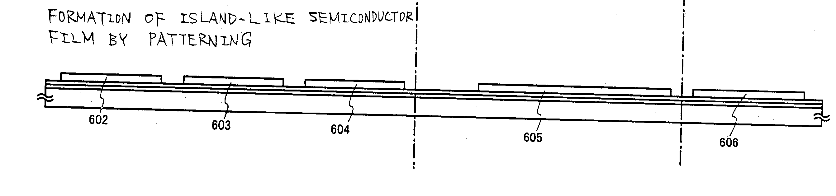
[0127] First of all, as shown in FIG. 12A, an amorphous semiconductor film is formed on an insulation surface, and then, the amorphous semiconductor film is subjected to an etching to form an island-like semiconductors 6001 and 6002. FIG. 12G is a top view of FIG. 12A, and a sectional view along the line A-A' is FIG. 12A. Then, as shown in FIG. 12B, an amorphous semiconductor film 6003 is formed to cover the island-like semiconductors 6001 and 6002. It is preferred that, immediately before forming the film, the film is subjected to rinse with diluted hydrofluoric acid to remove oxide film from the surface thereof, and then the amorphous semiconductor film 6003 is formed immediately. FIG. 12H is atop view of FIG. 12B, and a sectional view along the line A-A' is FIG. 12B.

[0128] Next, as shown in FIG. 12C, by subjecting the amorphous semiconductor film 6003...

example 3

[0131] Example 3 includes a process for crystallizing a semiconductor using a catalyst. Only the point, which is different from the Example 1, will be described. When a catalyst element is used, it is preferred to use the techniques, which are disclosed in Japanese Patent Laid-Open No. 7-130652 and in Japanese Patent Laid-Open No. 8-78329.

[0132] After forming the amorphous semiconductor film using Ni, the same is subjected to a solid-phase crystallization (hereinafter, the crystallization method will be referred to as NiSPC). For example, when the technique disclosed in Japanese Patent Laid-Open No. 7-130652, the amorphous semiconductor film is applied with solution of nickel acetate salt containing Nickel of 10 ppm in weight conversion to form a Nickel-containing layer, and after dehydrogenation processing for one hour at 500.degree. C., the same is subjected to a heat treatment for 4-12 hours at 500-650.degree. C.; for example, for 8 hours at 550.degree. C., to crystallize the sam...


PUM

PropertyMeasurementUnit
distanceaaaaaaaaaa
distanceaaaaaaaaaa
lengthaaaaaaaaaa

Abstract

Island-like semiconductor films and markers are formed prior to laser irradiation. Markers are used as positional references so as not to perform laser irradiation all over the semiconductor within a substrate surface, but to perform a minimum crystallization on at least indispensable portion. Since the time required for laser crystallization can be reduced, it is possible to increase the substrate processing speed. By applying the above-described constitution to a conventional SLS method, a means for solving such problem in the conventional SLS method that the substrate processing efficiency is insufficient, is provided.

Description

BACKGROUND OF THE INVENTION[0001] 1. Field of the Invention[0002] The present invention relates to a manufacturing method of semiconductor device having thin film transistor, particularly to a technique for forming crystalline semiconductor film, which comprises active layer of thin film transistor.[0003] 2. Related Art[0004] As a forming method of active layer on thin film transistor (Thin Film Transistor: hereinafter, referred to as TFT), a technique, in which an amorphous semiconductor film is formed on a substrate having an insulation surface, and then, crystallize the same in a manner of laser annealing or heat annealing, has been developed.[0005] The laser annealing is known as a crystallization technique, in which a high energy is given to an amorphous semiconductor film only without allowing the temperature of a glass substrate to rise too high, and thereby, the amorphous semiconductor film is crystallized. Particularly, excimer laser is a typical laser, which oscillates sho...

Claims


Application Information

Patent Timeline
Patent Type & Authority Applications(United States)
IPC IPC(8): G02F1/13H01L21/20H01L23/544
CPCH01L21/0237H01L21/02488H01L21/02532H01L21/02672H01L21/02686H01L23/544H01L27/1285H01L2223/54453H01L2924/0002H01L29/42384H01L2223/54426H01L2924/00G02F1/13
Inventor YAMAZAKI, SHUNPEISHIMOMURA, AKIHISAOHTANI, HISASHIHIROKI, MASAAKITANAKA, KOICHIROSHIGA, AIKOAKIBA, MAIKASAHARA, KENJI
Owner SEMICON ENERGY LAB CO LTD
Why Eureka
Try Eureka