Laser irradiation method and apparatus

Active Publication Date: 2006-01-10
SEMICON ENERGY LAB CO LTD
View PDF45 Cites 59 Cited by
  • Summary
  • Abstract
  • Description
  • Claims
  • Application Information

AI Technical Summary

Benefits of technology

[0014]By synthesizing the laser lights oscillated from the plurality of laser oscillating apparatuses, low energy density portions can complement each other in the laser lights. Thus, as compared with the case of using the laser lights emitted from the plurality of laser oscillating apparatuses independently without synthesizing the lights, an area of laser light having the energy density high enough for crystallization is expanded. As a result, a substrate processing efficiency can be enhanced.
[0015]Further, the present invention adopts a slit for partially cutting an area having the energy density below a predetermined level in the synthesized laser light in a scanning direction. With the above construction, an average value of energy densities of the laser light in the scanning direction can be increased and the laser light irradiation time per area is reduced. Further, despite t

Problems solved by technology

A glass substrate is inferior in heat resistance and is easily subjected to thermal deformation.
However, the small beam spot needs long scanning times of laser beam per one substrate, thereby the substrate proces

Method used


Image

  • Laser irradiation method and apparatus
  • Laser irradiation method and apparatus
  • Laser irradiation method and apparatus

Examples


embodiment 1

(Embodiment 1)

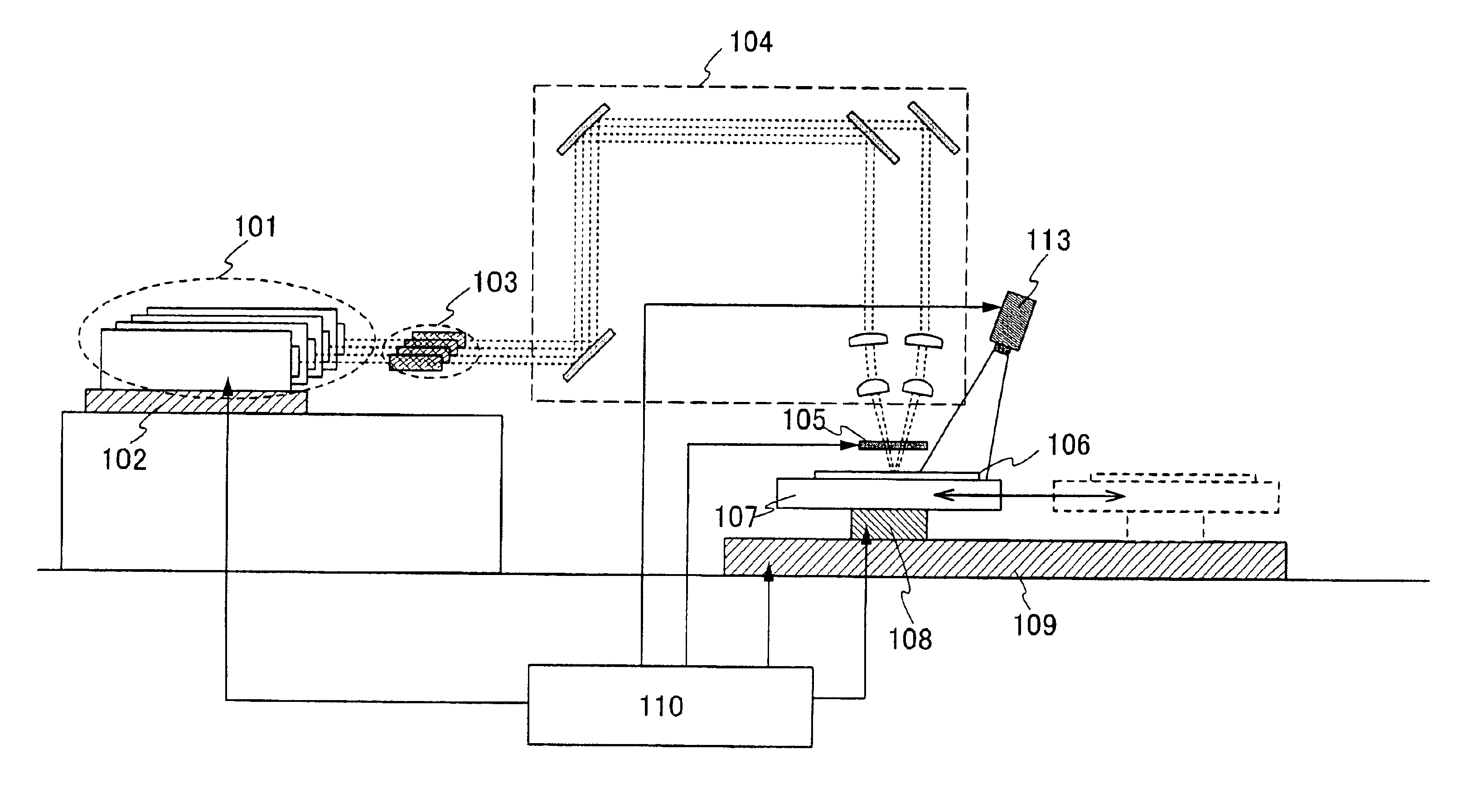
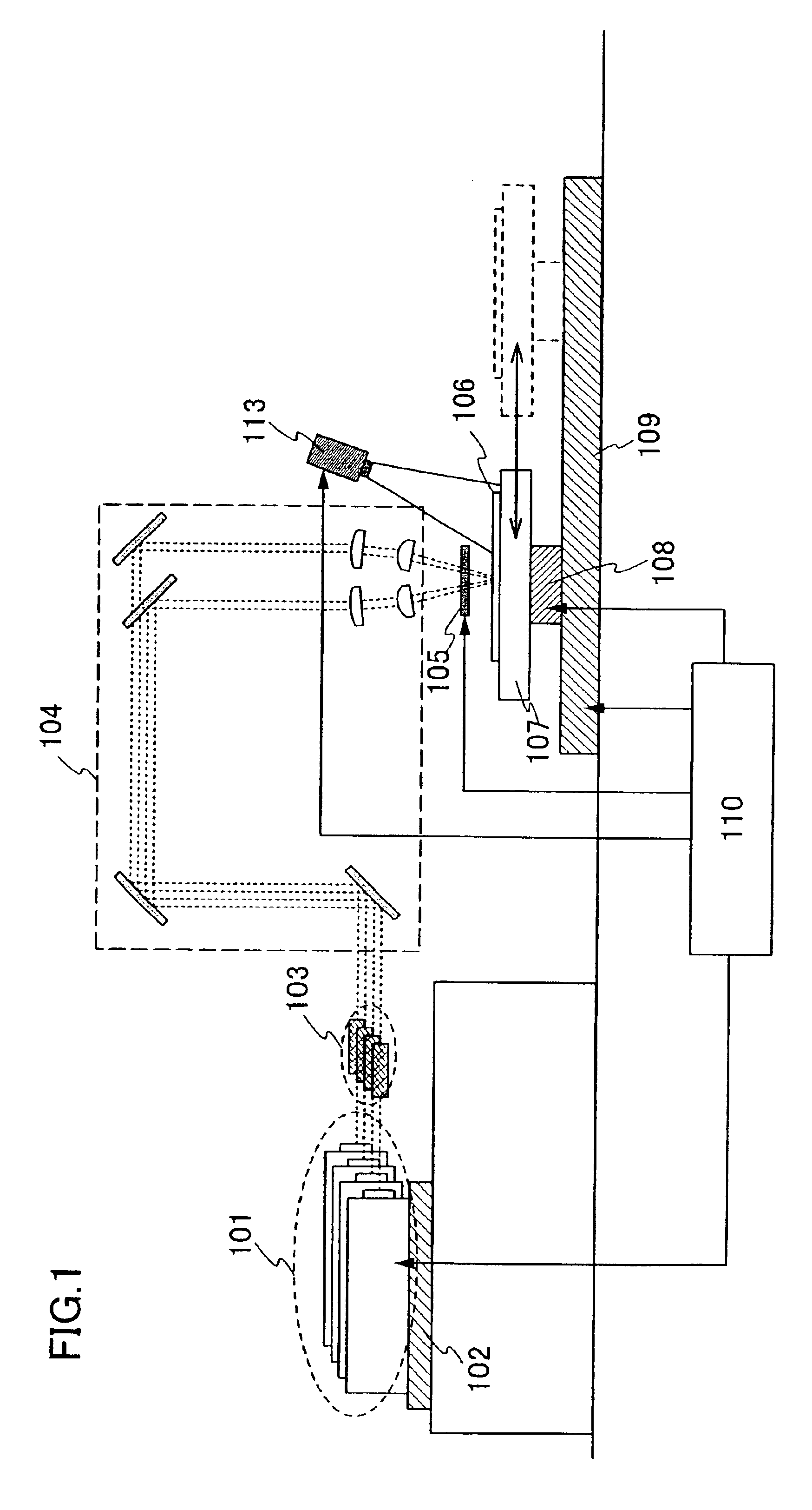
[0076]The crystalline semiconductor film formed by irradiation of laser light includes aggregations of a plurality of crystal grains. The crystal grains have random positions and sizes and hence, it is difficult to form a crystalline semiconductor film with specified positions and sizes of crystal grains. Accordingly, the active layers formed by patterning the crystalline semiconductor film into the islands may contain crystal grain interfaces (grain boundaries).

[0077]Unlike crystal grains, the grain boundaries contain therein an infinite number of recombination centers and trapping centers associated with amorphous structure and crystal defects. It is known that carriers trapped in the trapping centers increase the potential of the grain boundaries, which form barriers against carriers, so that the carriers are reduced in current transportability. Therefore, the grain boundaries present in the active layer of a TFT, or particularly in the channel forming region, will ...

embodiment 2

(Embodiment 2)

[0105]An optical system for overlapping beam spot will be described in this embodiment.

[0106]FIGS. 9A and 9B illustrate exemplary optical systems according to the embodiment. FIG. 9A shows a side view of an optical system of the laser irradiation apparatus of the present invention. FIG. 9B shows a side view that is viewed along the direction of the arrow B in the FIG. 9A. FIG. 9A shows a side view that is viewed along the direction of the arrow A in FIG. 9B.

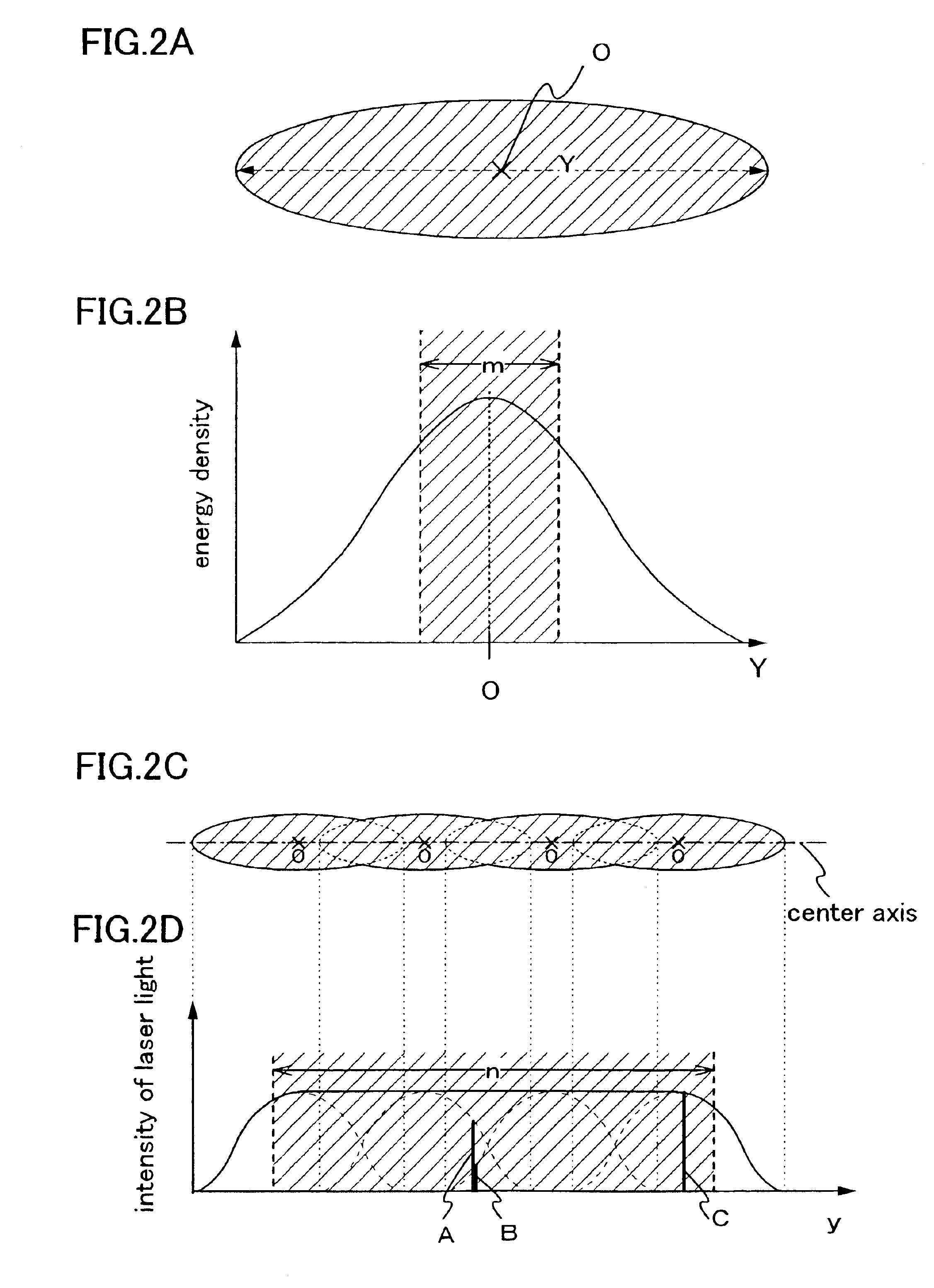
[0107]FIG. 9 shows an optical system which is adopted synthesize the four beam spots into a single beam spot. In this embodiment, the number of beam spot for synthesizing is not limited to this, the number may higher than or equal to 2 and lower than or equal to 8.

[0108]Reference numerals 401 to 405 are cylindrical lenses. The optical system of this embodiment includes six cylindrical-lenses, not shown in FIGS. 9A and 9B. FIG. 10 shows an oblique view of optical system shown in FIG. 9. Laser beam pass through the re...

embodiment 3

(Embodiment 3)

[0126]The manufacturing method of a semiconductor device using the laser irradiation apparatus or the laser irradiation method of the present invention will be described in this embodiment. Further, although a light emitting device is explained as one of the example of semiconductor device, the semiconductor device which can be manufactured by using the present invention is not limited thereto, a liquid crystal display device or other semiconductor devices can be applicable.

[0127]A light emitting device is the semiconductor device in which light emitting elements and means for applying current thereto are provided in each of plural pixels. An organic light emitting diode (OLED) has a layer including an electroluminescence material that generates an electroluminescence by applying an electric field (hereinafter, an electroluminescence layer), an anode layer, and a cathode layer. The electroluminescence layer is formed between the anode and the cathode and formed by sing...


PUM

PropertyMeasurementUnit
Angleaaaaaaaaaa
Angleaaaaaaaaaa
Pressureaaaaaaaaaa

Abstract

An objective of the present invention is to provide a laser crystallizing method capable of suppressing a thermal damage on a substrate as well as enhancing a substrate processing efficiency, and a laser irradiation apparatus using the laser crystallizing method. Laser lights oscillated from plural laser oscillating apparatuses are synthesized into one laser light and in a scanning direction of the laser light thus obtained, areas having an energy density lower than a predetermined level are cut with a slit. With the above construction, an average value of laser light energy densities can be increased in the scanning direction. Therefore, laser light irradiation time per area can be suppressed and in addition, a heat quantity applied to an object to be processed can be increased in total. Accordingly, a crystallinity of a semiconductor film can be increased while preventing the substrate from being excessively heated.

Description

BACKGROUND OF THE INVENTION[0001]1. Field of the Invention[0002]The present invention relates to a laser irradiation apparatus and a laser irradiation method for crystallizing a semiconductor film using a laser light or for performing activation after ion implantation.[0003]2. Description of the Related Art[0004]In recent years, a technique of forming a TFT on a substrate has greatly progressed, and its application and development for active matrix semiconductor display devices have been advanced. In particular, since a TFT Fusing a polycrystalline semiconductor film has higher field-effect mobility (also referred to as mobility) compared to a TFT using a conventional amorphous semiconductor film, it enables high-speed operation. Although the pixel is conventionally controlled by a driving circuit provided outside the substrate, it is therefore possible to control the pixel by the driving circuit formed on the same substrate where the pixel is formed.[0005]Incidentally, as for the s...

Claims


Application Information

Patent Timeline
IPC IPC(8): H01L21/00H01L21/20H01L21/84B23K26/06B23K26/073
CPCB23K26/0604B23K26/0608B23K26/0738B23K26/0732B23K26/0656B23K26/066
Inventor YAMAZAKI, SHUNPEITANAKA, KOICHIRO
Owner SEMICON ENERGY LAB CO LTD
Why Eureka
Try Eureka