
Raman-active taggants and thier recognition

a technology of raman photons and taggants, applied in the field of ramanactive taggants, can solve the problems of triply disadvantageous situation, ineffective raman scattering process, and only a fraction of the overall yield of raman photons

Inactive Publication Date: 2004-03-25
SHCHEGOLIKHIN ALEXANDER NIKITOVICH +4
View PDF2 Cites 138 Cited by
  • Summary
  • Abstract
  • Description
  • Claims
  • Application Information

AI Technical Summary

Benefits of technology

[0020] Of importance for comprehending aims, scope and advantages of the present invention is the fact that (as the patent of Chaney et al. Also surmises) there is no necessity always to provide Resonance Raman conditions to obtain good and useful Raman spectra of an analyte. Rather, Raman spectra of very high quality can be easily obtained also by using non-resonant or far from resonance excitations. In this case, however, the nature of a sample (i.e., whether this is an efficient Raman scatterer or not) is primarily responsible for whether intense or poor Raman spectrum will be produced. Hence, taking into account all the shortcomings of Resonance Raman spectroscopy noted above, it would be highly desirable to exploit an alternative approach based on normal Raman effect. The latter, however, although in principle being capable of providing more reliable, quantitative, practicable, simple and cost-effective means for detection of security features, automatically necessitates employment of intrinsically efficient Raman scatterers. Therefore, in accordance with the aims and scope of the present invention, there arises a substantial need for materials, coding compounds or taggants that would be intrinsically highly Raman-active, i.e. would have large Raman scattering cross sections and would be capable of producing intense Raman spectra under effect of characteristically non-resonant or far from resonance laser excitations.
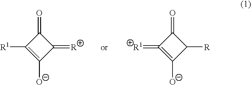
[0021] For the sake of better understanding aims, scope, novelty and advantages of the present invention it seems necessary to analyze in more details teachings of the U.S. Pat. No. 5,935,755 (Method for document marking and recognition, 1999, Kazmaier et al., Xerox Corporation) the disclosure of which is totally incorporated herein by reference. This document discloses numerous marking materials comprising the so called Raman-detectable compounds suitable for employment in printing inks and xerography toners for security applications such as authentication of documents. Particularly preferred Raman-detectable components are considered to be those that exhibit a distinct Raman spectrum at a wavelength where most paper and dye or pigment colorants are transparent. More particularly, it is stated that, when exposed to a Nd:YAG laser at 1064 nm, many squaraine compounds emit a strong, unique signal in the Raman spectrum at about 1600 cm.sup.-1 off the excitation laser line. Squaraine compounds preferred in the patent are of the general formula 1

Problems solved by technology

In principle, Raman scattering process is rather ineffective one.
However, even in best instance, the overall yield of Raman photons can reach only a fraction of a percent from the total amount of optical energy incident on the sample.
Thus, the one who intends to obtain a Raman spectrum of a conjugated polymer by virtue of RRS finds himself in triply disadvantageous situation.
Firstly, a considerable fraction of Raman photons unavoidably is lost due to their reabsorption by the sample itself (cf. FIGS. 15-16).
Secondly, a hypothetical possibility to pump more laser power into the sample, in order to generate more Raman photons, is not affordable in this case since there is always the risk to burn or otherwise destroy the sample.
And, thirdly, reasonable desire not to subject the sample to the risk for a long time too often means lowering the number of accumulated scans and, hence, a poorer SNR of the resulting spectrum.
The worst thing is that, when dealing with conjugated polymers or other intensely colored materials by RRS, the laser heating persistently changes the molecular structure of a sample during analysis.
Obviously, such mode of identification can not give precise results, since one has to analyze actually a sequence of several different samples (or a series of samples with differing molecular structure) during a single analysis!
At this point, however, the vibration is almost Raman-inactive, and more so at the higher temperatures.
ng role. Thus, those familiar with the art will probably agree that it is virtually impossible to predict the actual temperature of an intensely colored sample at different moments of time in the course of the RRS spectrum acquisition procedure (provided expensive or cumbersome special measures are not undertaken to stabilize the temperature of the
Usually, fluorescence emission is highly unwanted during Raman spectra acquisition.
With some upconverting phosphors, however, the Stokes LIF signal is represented by a limited number of well resolved spectral features.
The latter circumstance means that it would be difficult (if at all possible) task for a wrong-doer to identify this critical component in the mixture with organic taggants when attempting to analyze and / or reverse engineer the molecular code or label.
But without this fluorescing component present in infinitesimal quantities the molecular code will be incomplete for a Raman reader machine.
These individual modes are unstable with respect to one another and can render the device useless for precise quantitative analytical measurements.
Without such control, diode lasers are unstable and are thus generally regarded as of little use for Raman spectroscopic investigations.
Among their drawbacks also is that the wavelength of any diode laser device will gradually shift as the device ages.
A diode laser device, though stable for short times, is characterized by long-term instabilities which produce a slow drift, resulting in reduced instrument reliability.
Wavelengths beyond 900 nm adversely affect the detection capability of currently available multichannel detection systems (such as silicon CCDs).
In particular, it is extremely compact, rugged, rather sensitive and relatively inexpensive.
Although they are constantly improved and become less expensive, CCD detectors are still remain the most expensive component of the spectrometer.
Some CCD devices utilize a technology referred to as multi-pin phasing (MPP) which lowers background signal levels and noise to achieve desirable performance at temperatures lowered by air cooling, but these are still expensive.
Large-well devices consume large amounts of power and can get warm.
The Raman signals they measured were, however, very weak and obscure, so that their results seemed to suggest that the method might not be promising as a practical method unless we could intensify the Raman signals.
Therefore, even weak Raman peaks or background of the IRE can seriously interfere with measurements of supposedly rather weak Raman peaks produced by the evanescent wave from the sample surface.
Moreover, an increase in accuracy of electrical digital signal processing does not necessarily imply an increase in technological difficulties of its implementation, which is typical of optical analog signal processing.

Method used


Image

  • Raman-active taggants and thier recognition
  • Raman-active taggants and thier recognition
  • Raman-active taggants and thier recognition

Examples


example 1

[0194] General experimental setup I. A table-top system comprising a Perkin Elmer Corp. (Analytical Instruments, 761 Main Ave., Norwalk, Conn., 06859-0012 USA) NIR-FT Raman accessory fitted to a Perkin Elmer 1720 X FTIR spectrometer constituted the base of the first instrumental setup useful for accomplishing aims of the invention. The 1720X interferometer is furnished with a long-range KBr beam-splitter which gives a working range of between 370 and 10,000 cm.sup.-1. A specially stabilized Spectron SL-301 c / w Nd:YAG laser emitting at 1064 nm (9394 cm.sup.-1 TEM.sub.00 mode) manufactured by Spectron Laser Systems Ltd. (Rugby, UK) specifically for Perkin Elmer was used, providing between 2 mW and 3.5 W at the sample with a stability of 0.1% RMS. The sample optics employed is based on a 180.degree. back-scattering lens system (f / 0.6). The laser beam is directed on to the sample via a small prism, and its diameter at the sample position is approximately 0.5 mm. The scattered radiation ...

example 2

[0195] General experimental setup II. In another preferred embodiment of the invention, an alternative instrumental setup based on a miniature Raman spectrometer furnished with a fiber optic sampling probe was used for taking measurements directly "in the field". The complete system includes a S2000 miniature spectrometer manufactured by Ocean Optics Inc. (Dunedin, Fla. USA), an Enviva fiber optic Raman probe manufactured by Visionex Inc. (430 Tenth Street, N.W., Suite N205, Atlanta, Ga. 30318 USA) and, for example, an INF-780 single-mode AlGaAs diode laser manufactured by World Star Tech Inc.(Canada) as the main components. The S2000 spectrometer is based on a Czerny-Turner-type miniature spectrograph and has a Sony ILX511 noncooled rectangular reduction-type CCD linear image sensor as the detector. The sensor has 2048 pixels with a pixel size 14 .mu.m.times.200 .mu.m (14 .mu.m pitch) and maximum clock frequency 2 MHz. In accordance with aims of the invention, a 1200 lines / mm ruled...

example 3

[0196] General experimental setup III (Co-pending application possible). In another embodiment, an optional experimental setup has been devised and used for measuring thin-film prints produced in accordance with the present invention. To enhance detectability of the marks, patterns or images generated on a carrier in accordance with the invention, and thus now bearing a Raman-active compound of the invention (or a mixture thereof), a miniature waveguide Raman probe was used in frames of the general setup described in Example 2. More powerful 785-nm pigtailed diode laser module, for example, that manufactured by BWTec Inc., was used as an external excitation source in this setup. Such pigtailed single-mode laser gives up to 500 mW at the distal fiber end; the spectral bandwidth of the laser line to be about 1.2 nm HWFM. The exciting NIR laser beam was inserted through the end face of an internal reflection element (IRE) that had an appropriate end face angle, so that the refracted li...


PUM

PropertyMeasurementUnit
Raman shiftsaaaaaaaaaa
dimensionaaaaaaaaaa
wavelengthaaaaaaaaaa

Abstract

An organic or organoelement, linear or branched, monomeric or polymeric composition of matter having a Raman-active component in the form of particles. The particles having a maximum dimension of 50 mum. The Raman-active compound is applied to a substrate. When the Raman-active compound is exposed to a laser light wavelength which is batochromically well beyond a spectral region of maximum absorbance of said Raman-active compound, Raman scattering can be detected.

Description

[0001] The present invention pertains to the field of processes for prefatory anti-forgery protection and consecutive machine-assisted authentication of genuine documents and other values. More particularly, the invention pertains to the use of processes for authenticating security items with Raman spectroscopy. In particular, the present invention relates to improved Raman-active compounds and compositions thereof. In some embodiments the present invention relates to use of improved Raman-active compounds on documents and other security items in the form of visible, camouflaged or completely concealed prints and markings for the purposes of authentication. Further, the present invention relates to techniques of composing and placing security markings on the items which need to be protected against forgery or counterfeiting.[0002] Being directed, in some embodiments at least, to more reliable, facilitated, rapid and cost-effective mass authentication of genuine items "in the field" ...

Claims


Application Information

Patent Timeline
Patent Type & Authority Applications(United States)
IPC IPC(8): B41M3/14B41M5/28B44F1/12G01J3/44G01N21/65
CPCB41M3/14B41M3/144B41M5/285Y10S283/901G01J3/44G01N21/65G01N21/658B82Y30/00
Inventor SHCHEGOLIKHIN, ALEXANDER NIKITOVICHLAZAREVA, OLGA LEONIDOVNAMEL'NIKOV, VALERY PAVLOVICHOZERETSKI, VASSILI YUSMALL, LYLE DAVID
Owner SHCHEGOLIKHIN ALEXANDER NIKITOVICH
Learn More