Magnetoresistive sensor including magnetic domain control layers having high electric resistivity, magnetic head and magnetic disk apparatus
a magnetic domain control layer and magnetoresistive sensor technology, applied in the field of magnetoresistive sensors, can solve the problems of high loss of s/n of read sensor, difficult to ensure the insulating properties of the magnetic domain control layer, and difficult to provide a sufficient recording magnetic field for read elemen
- Summary
- Abstract
- Description
- Claims
- Application Information
AI Technical Summary
Benefits of technology
Problems solved by technology
Method used
Image
Examples
example 2
[0058] The magnetoresistive sensor in Example (1) described above has the structure by lamination from the lower portion. The structure in which the upper and lower portions are reversed can also give the same effect.
example 3
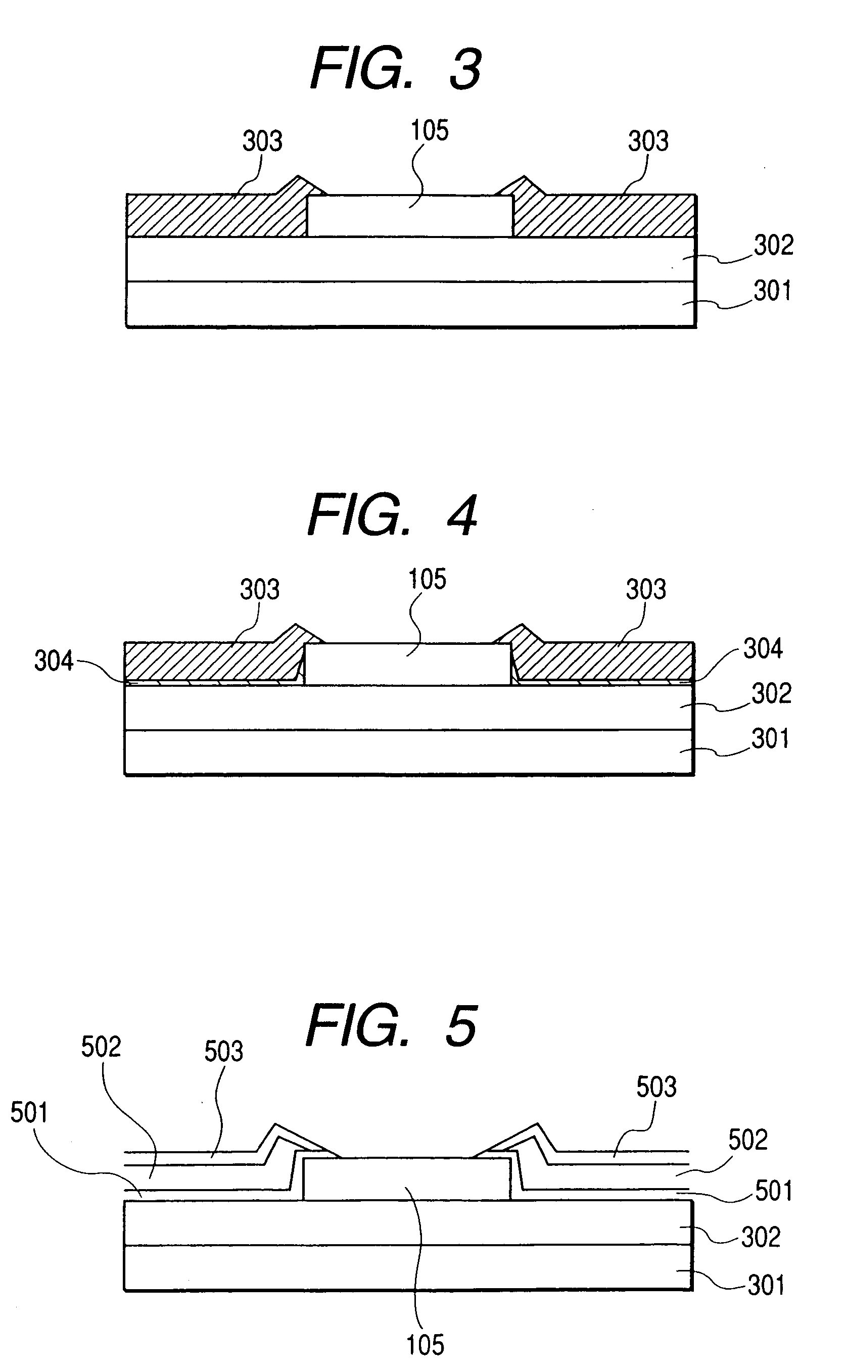
[0059] In Example (1) described above, in formation of the magnetic domain control layer using a spinel type oxide such as .gamma.-Fe2O3, on the underlayer 304 of the magnetic domain control layer 303, is formed, in place of the CoO layer, an oxide layer having a crystal structure of NaCl type such as Mg (200), NiO (200), EuO (200), FeO (200) or ZnO (200) as well as a (200) plane. Then, the spinel ferrite formed thereon can be crystallized at low temperature. As a method of forming this layer, there is a method of manufacturing these layers by the sputtering method, the ion beam sputtering method or the cluster ion beam method. As a method other than this, on the lower shied 302 a layer of Co, Mg, Ni, Eu, Fe or Zn is formed in a thickness of 1-5 nm. This layer is exposed to oxygen in vacuum, is irradiated with oxygen using ECR plasma, or is exposed to low-pressure oxygen by heating the substrate (100 to 250.degree. C.) so as to form an oxide layer, thereby forming a spinel ferrite t...
example 4
[0061] Before forming the magnetic domain control layer of Example 1 (1), as shown in FIG. 7, portions 701 are formed with MnZn ferrite as a soft magnetic layer having high electric resistivity, an insulator and a metal magnetic material are alternately laminated, or there is formed a granular layer in which these are sputtered at the same time into a mixed state, for example, a layer by laminating, by 25 number of layers, Co90Fe10 layers having a thickness of 1.4 nm and Al2O3 layers having a thickness of 1.0 nm. Thereafter, the outside of the layer is removed by the ion milling in the position several mm away from the outer peripheral portion of the magnetoresistive sensor layer, and then metal magnetic layers such as CoCrPt as represented by 502 are formed in the removed portions. This structure has no shunting since the metal magnetic domain control layers 502 are not in direct contact with the magnetoresistive sensor layer. However, since a layer with soft magnetic properties is...
PUM
 Abstract
Description
Claims
Application Information


