Electron-beam excitation laser

a laser and electron beam technology, applied in the field can solve the problems of low light emission efficiency of difficult to cause laser oscillation by current injection, and high oscillation threshold value of conventional electron beam excitation lasers

Inactive Publication Date: 2004-11-04
CANON KK
View PDF25 Cites 61 Cited by
  • Summary
  • Abstract
  • Description
  • Claims
  • Application Information

AI Technical Summary

Problems solved by technology

The light is caused to reciprocate many times to be progressively amplified thereby cause laser oscillation.
However, it is difficult to cause laser oscillation by current injection, using a wide-band-gap semiconductor because of its electrical characteristics, such as the fact that such a semiconductor cannot freely be doped.
(1) Conventional electron-beam excitation lasers are low in light emission efficiency and high in oscillation threshold value. Laser oscillation occurs over a wide wavelength region in various modes.
(2) When a thick reflecting layer is provided so that its side to which an electron beam is irradiated has sufficient light reflecting capability, an electron beam attenuates by the time it reaches the active layer, thus lowering light emission efficiency. To prevent such a reduction in light emission efficiency, electron-beam accelerating voltage must be increased.
(3) Because a laser structure (a semiconductor layer) is made by vapor-phase growth methods, such as MBE and CBE, the structure is costly, so that lasers using such a structure are difficult to offer at low cost.
These defects cause local disorder in the photonic crystal, so that the oscillation threshold value becomes smaller, thus easily providing laser oscillation in a single mode.
(1) Using a photonic band gap in a multidimensional photonic crystal for a reflector makes high-level light reflection and containment possible. This allows oscillation to easily occur in a single mode within a narrow frequency range and light emission anisotropy to be controlled using photonic-crystal multidimensionality.
(2) Periodically disposing a light-emitting material in a multidimensional photonic crystal increases light emission efficiency and reduces the oscillation threshold value. This is reasoned as follows. A photonic crystal allows an optical mode in which group velocity is low to be entered. Time of interaction between a material system and a radiation field is inversely proportional to group velocity. Thus a group velocity reduction is used to increase the amplification factor (O Plus E, Vol. 21, p.
(3) Introducing local disorder, that is, defects into a photonic crystal allows a mode in which light exists locally in a photonic band gap to be entered. If a light-emitting frequency is in the photonic band gap, spontaneous light emission and inductive light emission are prohibited because no optical mode in which light is emitted is available at frequencies other than frequencies in the above-described mode. Using such a photonic crystal with defects for a light emitter or a reflector causes the above-described mode to be entered, the frequency range for light emission and laser oscillation to be narrowed, and time and space coherence to be increased. This makes it easy to cause laser oscillation in a single mode at a low threshold value.
However, the crystal is difficult to produce, it does not find wide application.
Because a periodic structure several hundreds of nanometers in size needs to be formed to make a photonic crystal which emits light in the visible region, the crystal is difficult to make.
However, because these techniques pose problems of a poor yield, high cost, and so on, a spontaneously formed regular nanostructure is preferably used.

Method used


Image

  • Electron-beam excitation laser
  • Electron-beam excitation laser
  • Electron-beam excitation laser

Examples


embodiment 1

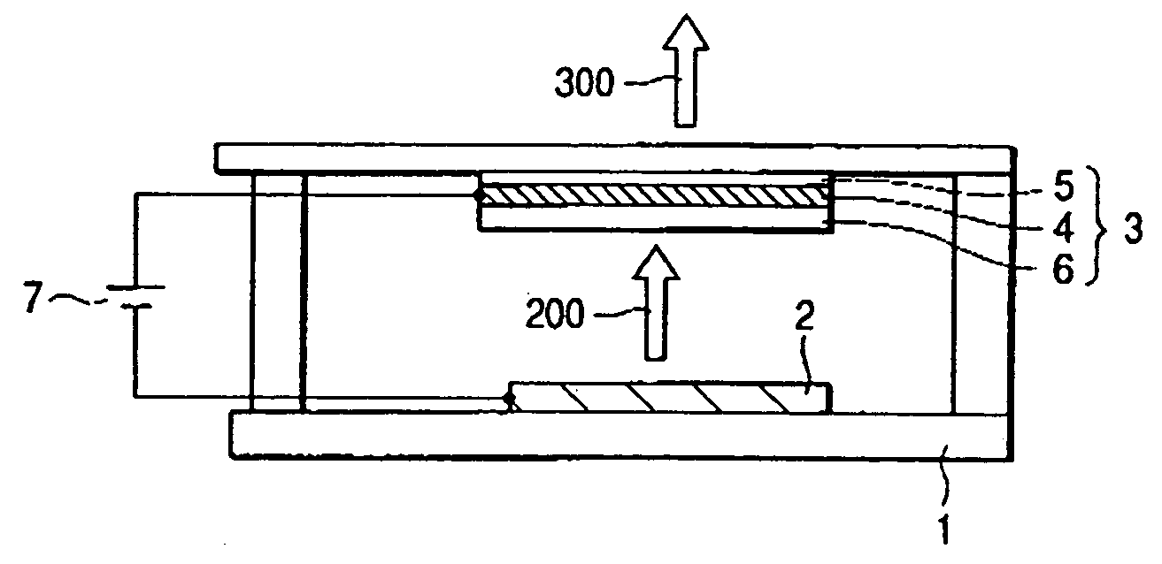
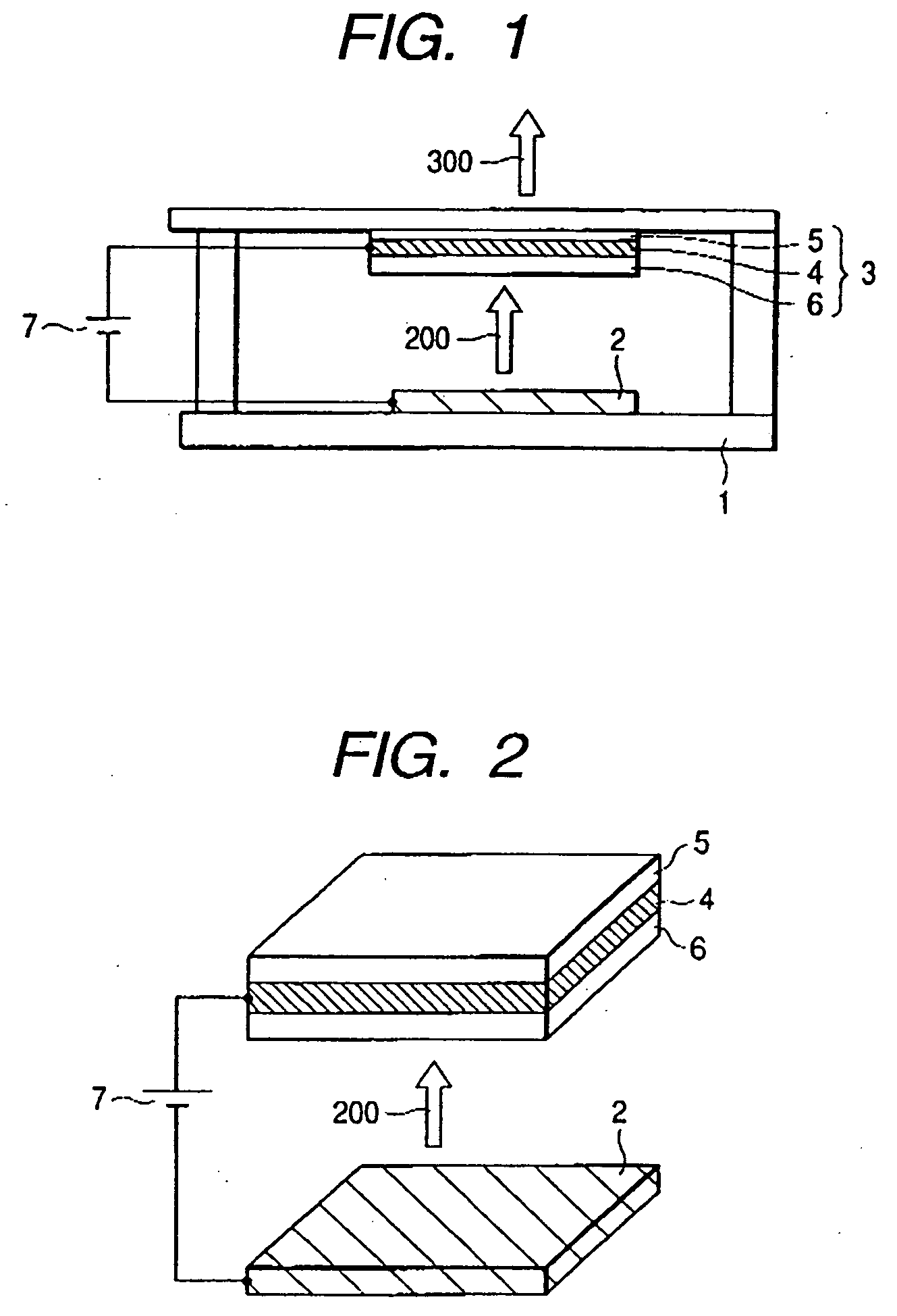
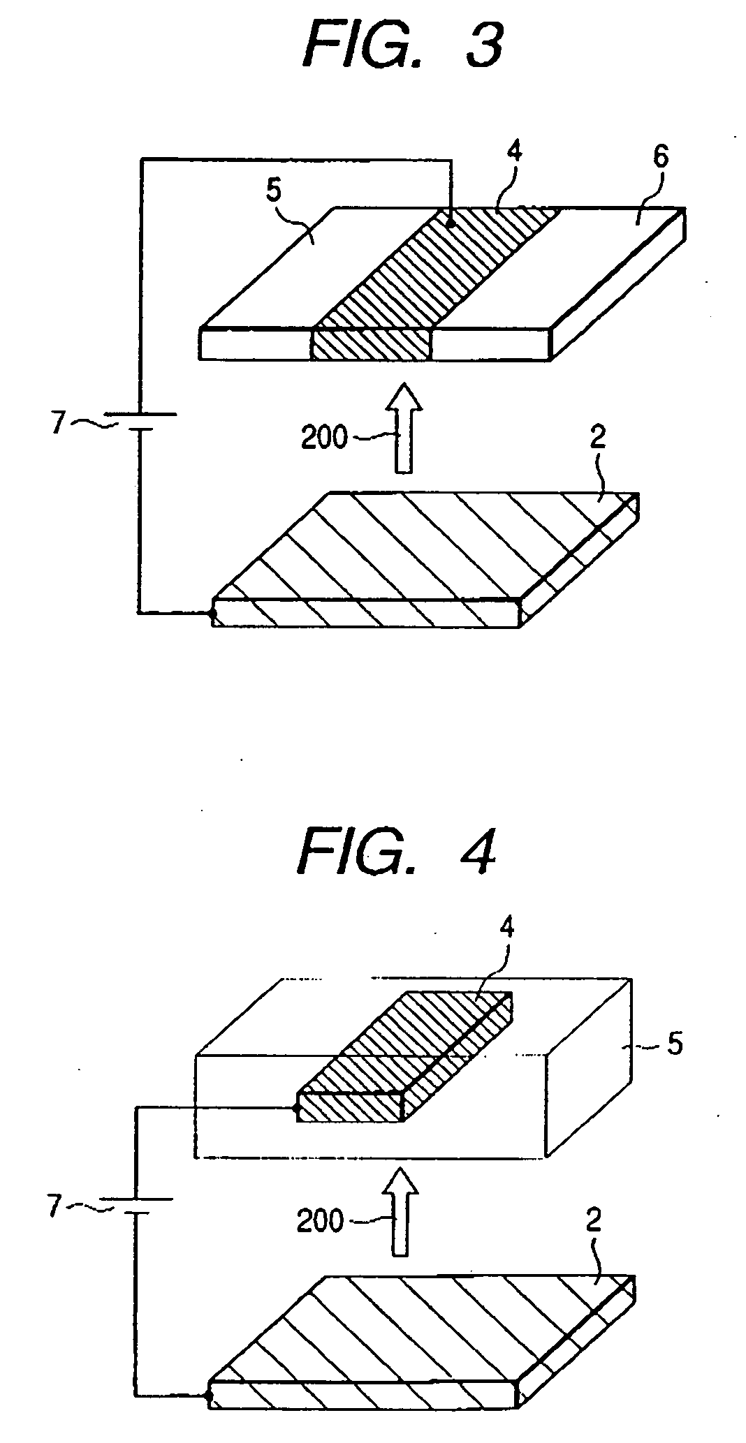
[0078] Specifically, Nb film 100 nm thick was formed on a quartz substrate, then aluminum film 1 .mu.m thick was formed on the Nb film by DC sputtering. Next, as is the case with Embodiment 1, the aluminum film was anodized to make alumina nanoholes. These nanoholes were formed at 140 nm intervals in honeycomb formation. Then the aluminum film was anodized at 56 V, using a 0.3M phosphoric acid bath. Finally, the film was subjected to pore wide treatment, that is, immersed in a 5 wt % phosphoric acid solution at 25.degree. C. for 50 minutes to enlarge nanoholes until their diameter reached about 110 nm.

[0079] By electrodeposition, the nanoholes were filled with ZnO to make a light emitter. The substrate was immersed in a 0.1M zinc nitrate solution at 60.degree. C. together with an opposite Pt electrode. Next, a voltage of about -5 V was applied to the substrate to form ZnO crystals in the nanoholes. In Embodiment 7, ZnO crystals were let to grow until they protruded from the nanohole...

embodiment 11

[0084] In Embodiment 11, a laser structure which uses a GRINSH (graded index separate confinement) type ZnCdSe / ZnSe heterostructure produced by MBE for a light emitter was made and evaluated. The laser structure corresponds to FIG. 12A. The light emitter has a heterostructure. The heterostructure consists of a 1 .mu.m thick ZnSe buffer layer on an InGaAs (100) substrate and a quantum well which is made from Zn.sub.0.75Cd.sub.0.25Se interposed between refractive-index change layers of Zn1-xCdxSe (x=0 to 0.05) and is disposed on top of the buffer layer. The refractive-index change layer is 500 nm thick.

embodiment 2

[0085] A reflector made from anodized alumina was formed on the heterostructure in the same was to make the laser structure. In the embodiment, start points were arrayed at 170-nm intervals in honeycomb formation, and anodization was performed at 68 V in a 0.3M phosphoric acid bath. Finally, the laser structure was subjected to pore wide treatment, that is, immersed in a 5 wt % phosphoric acid solution at 25.degree. C. for 70 minutes to enlarge nanoholes until their diameter reached about 140 nm.

[0086] A spint type electron source was provided which has 10.sup.4 to 10.sup.5 Mo chips per square millimeter. The thus produced laser structure was placed opposite to the spint type electron source in a glass container. After the container was evacuated, it was hermetically sealed. As electron accelerating means, a high-voltage power supply was connected to the electron source and laser structure. When a beam of electrons accelerated to an acceleration voltage of 10 to 50 keV was irradiat...


PUM


Abstract

An electron-beam excitation laser has a laser structure with a light emitter and reflectors on one hand and an electron source on the other hand, wherein at least part of the light emitter or reflectors has a multidimensional photonic crystal structure. An electron-beam excitation laser includes an electron source emitting electrons and a laser structure consisting of a light emitter and reflectors, accelerates electrons from the electron source, and irradiates the electrons to the laser structure to emit a laser beam from the laser structure, wherein the reflectors and / or the light emitter in the laser structure are formed with multidimensional photonic crystals in which dielectrics with different dielectric constants are arrayed in a plurality of directions at periodic intervals, and one of the dielectrics with different dielectric constants may be formed with a light-emitting material.

Description

[0001] 1. Field of the Invention[0002] The present invention relates to an electron-beam excitation laser, and more particularly, to an electron-beam excitation laser emitting light distributed from the visible region to the ultraviolet region. An electron-beam excitation laser according to the present invention can be used as a light source for a laser beam printer, an optical recorder, optical communications, a pointer, a display, and so on.[0003] 2. Related Background Art[0004] A laser consists commonly of a laser medium, a resonator including a reflector, and an excitation source. A laser medium obtains energy from an excitation source to emit light with a specific wavelength, so that a laser beam is generated in a state that allows amplification with gain. An optical resonator reflects light emitted by the laser medium to return it to the medium. The light is caused to reciprocate many times to be progressively amplified thereby cause laser oscillation. Lasers come in various t...

Claims


Application Information

Patent Timeline
Patent Type & Authority Applications(United States)
IPC IPC(8): G02B5/18H01J29/10H01J31/10H01S3/08H01S3/0959H01S3/16H01S5/022H01S5/04H01S5/30
CPCH01S3/0959H01S5/02208H01S5/0222H01S5/04H01S5/105H01S5/183H01S5/3018H01S5/423H01S5/11
Inventor IWASAKI, TATSUYADEN, TOHRU
Owner CANON KK
Why Eureka
Try Eureka