Probe structures incorporating nanowhiskers, production methods thereof and methods of forming nanowhiskers

a technology of nanowhiskers and nanowires, which is applied in the direction of material analysis using wave/particle radiation, instruments, nuclear engineering, etc., can solve the problems of spm-tips suffering from the same limitation as conventional metallic spm-tips, and the efficient injection of spin-polarised electrons into spintronic devices, etc., to reduce the size of a ferromagnetic domain formed, reduce the symmetry of nanowires, and improve the curie temperature of magnetic semiconductor materials

Inactive Publication Date: 2005-01-27
QUNANO
View PDF34 Cites 103 Cited by
  • Summary
  • Abstract
  • Description
  • Claims
  • Application Information

AI Technical Summary

Benefits of technology

[0041] With regard to ferromagnetic properties, nanowhiskers may present a possibility for retaining ferromagnetism in very small regions. There is much interest in magnetic memory devices employing very small, typically single-domain, magnetic particles, or similar structures, as memory elements. However, it is known that as the size of a ferromagnetic single domain is reduced a limit is reached below which the ferromagnetic state cannot exist, and the domain, e.g., the single particle, assumes the superparamagnetic state in which the magnetic moments of all the atoms still line up to form the collective huge magnetic moment as in a ferromagnet, but where the orientation of this huge spin is no longer locked into a defined direction as it is in a ferromagnet. This limit is typically about 50 nm for a spherical magnetic particle. However, when a magnetic domain, e.g., a ferromagnetic domain, is incorporated into a nanowhisker, the diameter at which the domain ceases to be ferromagnetic and undergoes a transition to the superparamagnetic state can be reduced, because the substantially one-dimensional character of the nanowhisker tends to restrict the possible reorientation of the magnetic moment of the ions (or atoms) of the magnetic material. The material of the whisk

Problems solved by technology

However, adhesive may fail, particularly when the SPM is immersed in fluid.
Furthermore, such SPM-tips will, in principle, suffer from the same limitation as a conventional metallic SPM-tip, with the si

Method used


Image

  • Probe structures incorporating nanowhiskers, production methods thereof and methods of forming nanowhiskers
  • Probe structures incorporating nanowhiskers, production methods thereof and methods of forming nanowhiskers
  • Probe structures incorporating nanowhiskers, production methods thereof and methods of forming nanowhiskers

Examples


second embodiment

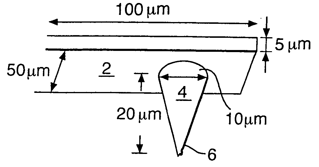
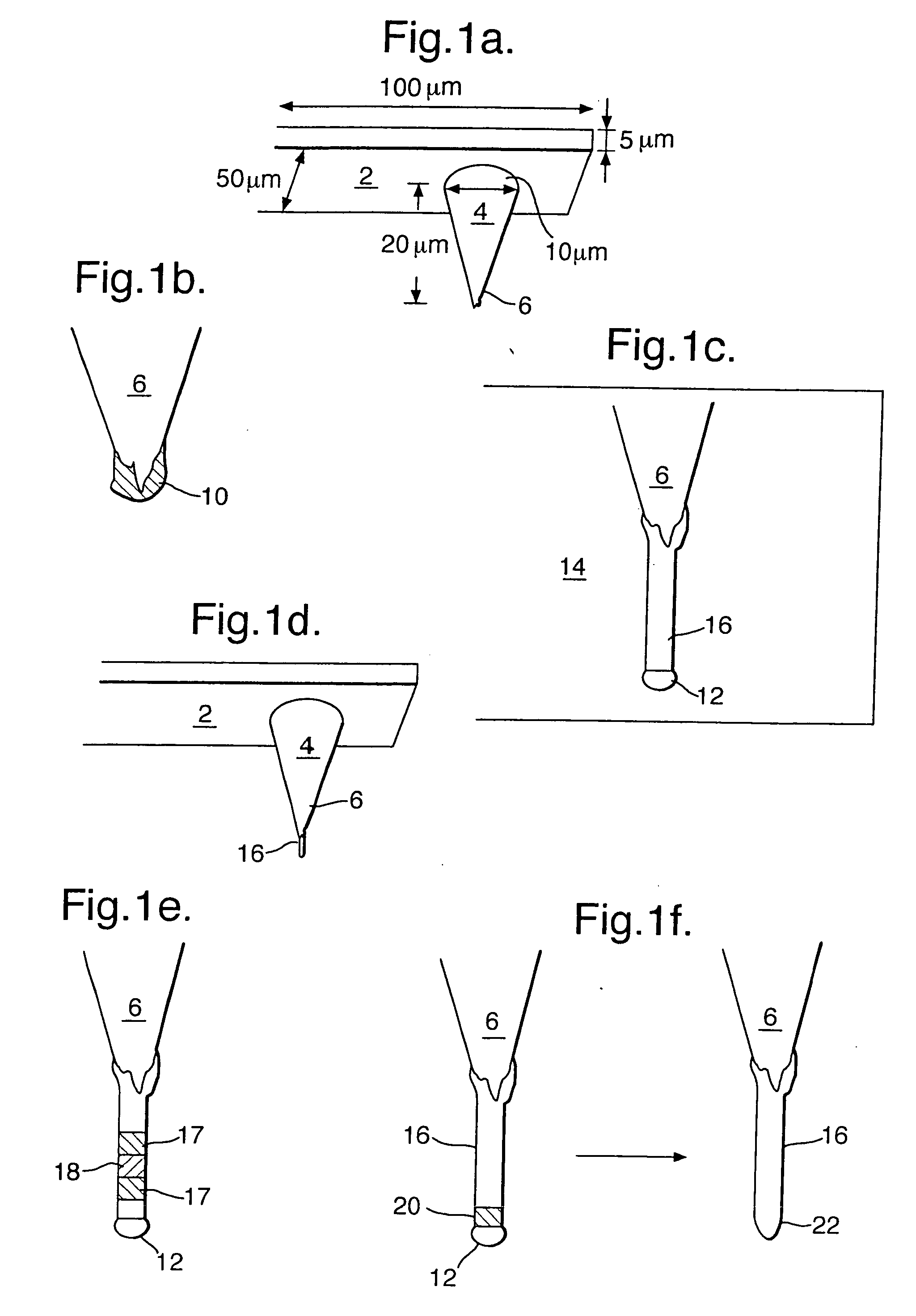
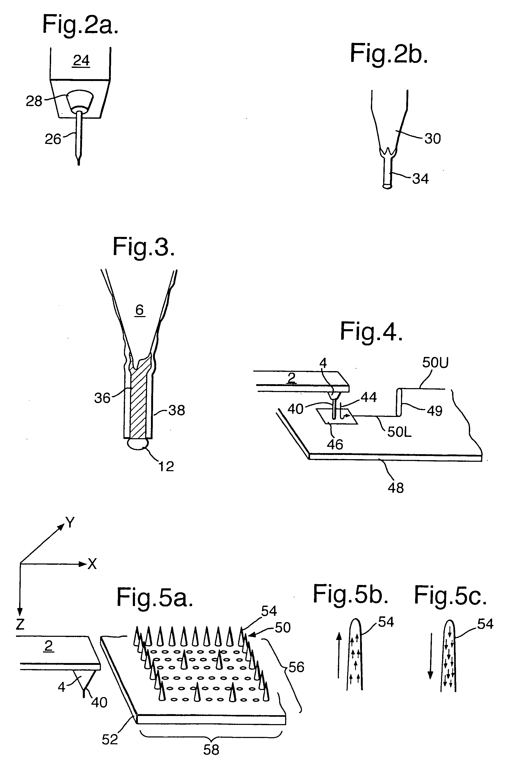
[0065]FIGS. 2 and 2b show a probe for an STM according to the invention. In FIG. 2a, a support 24 mounts an STM tip structure comprising a metallic wire tip member 26 held in a holder 28. The end of the wire 26, as shown in FIG. 2b, is tapered as at 30. A nanowhisker 34 is formed at the end, in accordance with the processes described above with reference to FIGS. 1b to 1g. Since STM applications usually require measurements of an atomic scale, the nanowhisker may have a very small diameter, at least at its tip, say 10 nm or less, or even less than 5 nm.

third embodiment

[0066] Referring now to FIG. 3, a third embodiment is shown comprising a tip structure of an AFM, with integral nanowhisker, where similar parts to those of FIG. 1 are denoted by the same reference numerals. A nanowhisker 36 is formed by the method described above. The whisker is formed of silicon and has a gold particle melt 12 at one end. Subsequent to formation of the whisker, the whisker is exposed to an atmosphere at a suitable temperature for oxidation of the silicon. This forms an outer shell 38 of silicon dioxide surrounding the whisker and extending along its length. The gold particle melt 38 remains in an unoxidised condition.

[0067] This therefore provides a structure highly suitable for precise examination of biological samples, since the region of interaction with the biological sample is very precisely defined. The nanowhisker 36, 38, 12 may be used, for example, to map properties of biological tissue in three directions of movement of the tip structure, X, Y, Z.

[0068]...

fourth embodiment

[0070] Referring now to FIG. 4, the invention is shown for use in the field of Spintronics. Spintronics is a technical field where the properties of electronic devices rely on the transport of electron spin through the device. In FIG. 4 similar parts to those of FIG. 1 are denoted by similar reference numerals. A whisker 40, formed at the end of the tip member 4, by the process described above, is of a magnetic material (MnInAs, MnGaAs, MnAs) or semimagnetic material, containing a dilute concentration of Mn. Under an applied voltage V, spin polarised electrons 44 are emitted from the tip of the whisker, which makes electrical contact with an electrical contact 46 disposed on a substrate 48. The spin polarised electrons 44 are injected by means of a tunnelling process into contact 46 and are then used for a desired function, such as reading the state of a magnetic memory element, such as nanopillar 49 disposed on substrate 48 and electrically connected by means of lower and upper ele...


PUM


Abstract

A probe structure for a scanning probe microscope comprises a nanowhisker (16,34) projecting from a free end of an upstanding tip member (4,26), and being formed integrally with the tip member. In another embodiment, a data storage medium comprises an array of nanowhiskers (54), each nanowhisker being formed from magnetic material, the diameter of the nanowhisker being such that a single ferromagnetic domain exists within the nanowhisker, preferably having a diameter not greater than about 25 nm and more preferably not greater than about 10 nm, and a read/write structure comprising the probe structure for injecting a stream of spin-polarised electrons into a selected nanowhisker of the array, either for sensing the direction of magnetisation in the nanowhisker, or for forcing the nanowhisker into a desired direction of magnetisation. When the probe nanowhisker is formed by a VLS process using a catalytic particle melt, the whisker may be formed with a sacrificial segment to allow for removal of the catalytic material by selective etching of the segment.

Description

CROSS-REFERENCE TO RELATED APPLICATION [0001] This application claims the benefit of U.S. Provisional Application No. 60 / 485,104 filed Jul. 8, 2003, which is incorporated herein by reference.FIELD OF THE INVENTION [0002] The present invention relates to structures, incorporating one-dimensional nanoelements and which are suitable for use in scanning probe microscopy, current injection applications, and other applications. “One-dimensional nanoelements” are structures, essentially in one-dimensional form, that are of nanometer dimensions in their width or diameter, and which are commonly known as nanowhiskers, nanorods, nanowires, nanotubes, etc. More specifically, but not exclusively, the invention is concerned with structures incorporating nanowhiskers, related production methods, and to methods of forming nanowhiskers. BACKGROUND ART [0003] The basic process of whisker formation on substrates, by the so-called VLS (Vapour-Liquid-Solid) mechanism is well known. A particle or mass o...

Claims


Application Information

Patent Timeline
IPC IPC(8): D01F9/08G01N23/00G01Q70/12G01Q70/16
CPCB82Y15/00B82Y35/00G01Q70/12G01Q60/54D01F9/08G01Q60/48
Inventor SAMUELSON, LARS IVAROHLSSON, BJORN JONAS
Owner QUNANO
Why Eureka
Try Eureka