Semiconductor device and manufacturing method thereof

a technology of semiconductors and semiconductors, applied in the direction of sustainable manufacturing/processing, instruments, final product manufacturing, etc., can solve the problems of unmanufactured tft compared with one formed on glass substrates, difficult to obtain uniform display, and liable to occur signal delays

Inactive Publication Date: 2005-01-27
SEMICON ENERGY LAB CO LTD
View PDF22 Cites 90 Cited by
  • Summary
  • Abstract
  • Description
  • Claims
  • Application Information

AI Technical Summary

Benefits of technology

[0213] According to the present invention, since a substrate (an element forming substrate) having a higher heat resistance than that of plastic is used in the manufacturing process of a semiconductor element, a semiconductor element having excellent electric characteristics can be manufactured. Further, since the element forming substrate is detached after a semiconductor element and a light emitting element are formed and is attached to a plastic support.
[0214] Therefore, it is made possible to use a plastic support as the supporting substrate and to manufacture a high performance electric device. Further, since the supporting substrate is plastic, the electric device can be made flexible and light in weight.
[0215] Further, by providing color filters between an underlayer film having the semiconductor element and the light emitting element provided thereon and a plastic support, not only is color display accomplished but also the color filters can function as a light shielding film, and thus the reliability of the device can be improved.

Problems solved by technology

However, the present situation is that a satisfactory TFT compared with one formed on a glass substrate has not been manufactured as vet.
Since, in this way, a light emitting element itself has the ability of emitting light in an EL display device, a backlight which is used in a liquid crystal display device is unnecessary.
In an EL display device where EL elements emitting red, green, and blue colors are used, since different EL materials are used to form EL elements emitting the respective colors, the element characteristics differ accordingly, and it is difficult to obtain uniform display.
Also, a liquid crystal device using a metal film as the light shielding mask has a problem that signal delays are liable to occur due to parasitic capacitance formed between the metal film and other wirings.
A liquid crystal device using an organic film to insulate the light shielding mask from other wirings has a problem that the number of the manufacturing processes increases.

Method used


Image

  • Semiconductor device and manufacturing method thereof
  • Semiconductor device and manufacturing method thereof
  • Semiconductor device and manufacturing method thereof

Examples


embodiment

[0055] (Embodiment Mode 1)

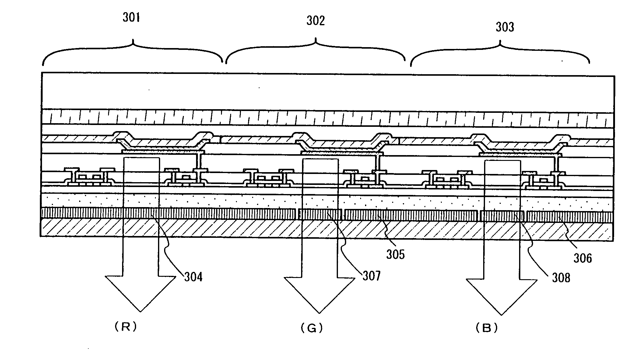
[0056]FIG. 1 illustrates an EL display device according to the present invention.

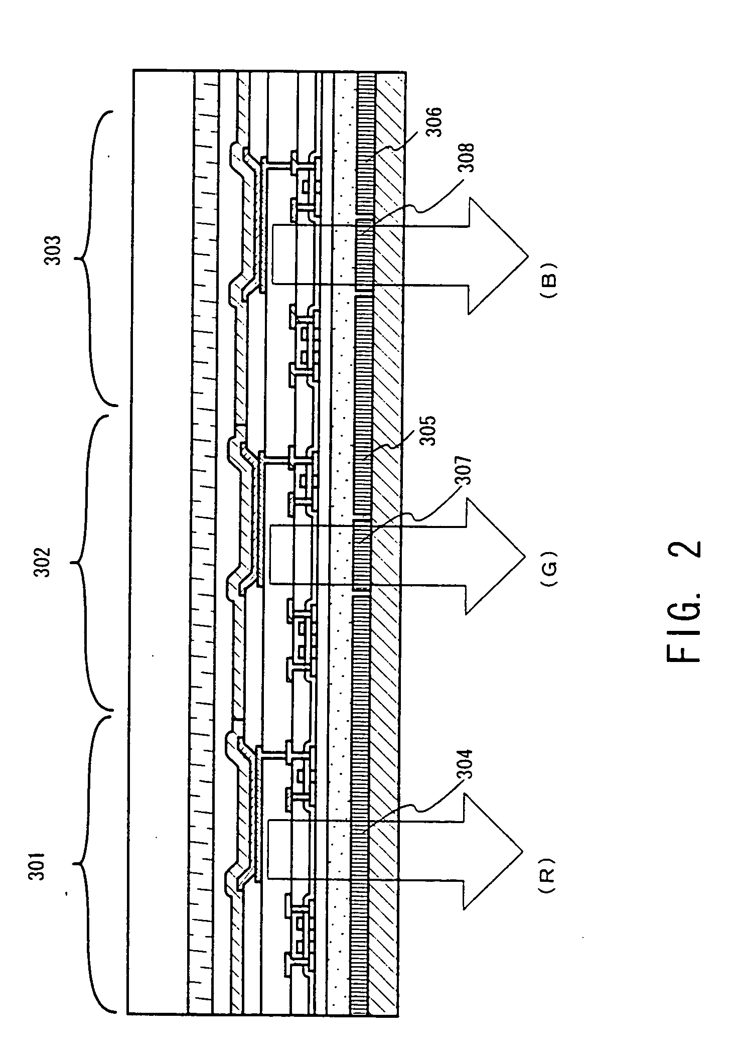
[0057] An underlayer film 12 is attached to a plastic substrate (a second substrate) 11 using a second adhesive layer 58. A switching TFT 201 and a current controlling TFT 202 for forming a pixel portion, and an p-channel TFT 205 and a n-channel TFT 204 forming a driver circuit are provided on the underlayer film 12. It is to be noted that the respective TFTs include an active layer of the respective TFTs (including the channel forming regions 17a, 17b, 29, 38, and 42, source regions 13, 26, 35, and 40, drain regions 14, 27, 36, and 41, and LDD regions 15a, 15b, 15c, 15d, and 37), a gate insulating film 18 covering the active layer, gate electrodes 19a, 19b, 30, 39, and 43 aligned with the channel forming regions through the gate insulating film, a first 15 interlayer insulating film 20 covering the gate electrodes, source wirings 21, 31, 44, and 45 and drain wirings 22, 32, a...

embodiment 1

[0075] [Embodiment 1]

[0076] An embodiment according to the present invention is described with reference to FIGS. 4 to 7. Here, a method of simultaneously forming on a first substrate 500, TFTs in a pixel portion and TFTs in a driver circuit portion provided on the periphery of the pixel portion is described. It is to be noted that, for the sake of simplicity, a CMOS circuit as a basic unit is illustrated with regard to the driver circuit.

[0077] In FIG. 4A, a separating layer 501a comprising an amorphous silicon film at the thickness of 100 to 500 nm (300 nm in the present embodiment) is formed on a substrate 500 where elements are to be formed (hereinafter referred to as an element forming substrate). Though a glass substrate is used in the present embodiment as the element forming substrate (the first substrate) 500, a quartz substrate, a silicon substrate, a metal substrate, or a ceramic substrate may also be used. It is to be noted that the substrate having a semiconductor elem...

embodiment 2

[0124] [Embodiment 2]

[0125] In the present example, a process for moving to a plastic substrate the TFTs and the EL elements formed on the first substrate according to Embodiment 1 after the processes in Example 1 is described with reference to FIGS. 8 and 9.

[0126] First, according to Embodiment 1, the structure illustrated in FIG. 7C is obtained. It is to be noted that, in the present embodiment, since color filters are used. EL elements provided with an organic EL layer emitting white light are used. More specifically, as the light emission layer, a material disclosed in Japanese Patent Application Laid-open Nos. Hei 8-96959 or Hei 9-63770 may be used. In the present embodiment, as the light emission layer, 1,2-dichloromethane with PVK (polyvinyl carbazole), Bu-PBD (2-(4′-tert-butylphenyl)-5-(4″-biphenyl)-1,3,4-oxadiazole), coumarin 6, DCM1 (4-dicyanomethylene-2-methyl-6-p-dimethylaminostyril-4H-pyran), TPB (tetraphenyl butadiene), and Nile red dissolved therein is used.

[0127] I...


PUM

PropertyMeasurementUnit
thicknessaaaaaaaaaa
thicknessaaaaaaaaaa
thicknessaaaaaaaaaa

Abstract

A high performance electric device which uses an adhesive layer over a substrate. A color filter is over a substrate, and an adhesive layer is also located over the substrate and color film. An insulating layer is over the adhesive layer, and thin film transistors cover the insulating film and the color filters. Light emitting elements cover the thin film transistors and emit light through the substrate that is through the adhesive layer and color filter. The substrate may be plastic, thus increasing the heat resistance.

Description

BACKGROUND OF THE INVENTION [0001] 1. Field of the Invention [0002] The present invention relates to a semiconductor device which includes therein a device (hereinafter referred to as a light emitting device) having an element where a light emitting material is sandwiched between electrodes (hereinafter referred to as a light emitting element) or a device (hereinafter referred to as a liquid crystal display device or a liquid crystal module) having an element where liquid crystal is sandwiched between electrodes (hereinafter referred to as a liquid crystal element), and a method of manufacturing thereof. For example, the present invention relates to an electric device represented by a liquid crystal display device and a light emitting device, and to an electronic equipment (electronic apparatus) having such an electric device (electronic device) mounted thereon as a component. [0003] It is to be noted that, as used herein, the term “semiconductor device” refers to any device which c...

Claims


Application Information

Patent Timeline
Patent Type & Authority Applications(United States)
IPC IPC(8): G02F1/1333G02F1/1335G02F1/1362H01L21/77H01L21/84G02F1/136H01L27/32H01L51/52H01L51/56H05B44/00
CPCG02F1/133305H01L51/0097G02F1/13454G02F1/136227G02F2001/13613G02F2202/104H01L27/1214H01L27/1266H01L27/322H01L27/3244H01L27/3246H01L27/3272H01L27/3276H01L51/001H01L51/003H01L51/5237H01L51/5284H01L51/56H01L2221/68363H01L2227/326H01L2251/5338H01L27/1218G02F1/1368G02F1/13624H01L27/3262H01L27/124G02F2001/136222G02F1/133516Y02E10/549G02F1/13613Y02P70/50H10K59/38H10K59/122H10K59/12H10K59/126H10K71/164H10K59/131H10K71/80H10K50/841H10K50/844H10K50/865H10K59/1201H10K2102/311H10K71/00G02F1/136G02F1/136222H10K59/1213H10K77/111H10K50/84G02F1/133514G02F1/134309
Inventor YAMAZAKI, SHUNPEI
Owner SEMICON ENERGY LAB CO LTD
Why Eureka
Try Eureka