Methods for fabricating a substrate

a substrate and method technology, applied in the direction of polycrystalline material growth, crystal growth process, chemically reactive gas, etc., can solve the problems of not being able to obtain or otherwise not available, unable not being able to meet the requirements of a working layer,

Inactive Publication Date: 2005-02-03
SOITEC SA
View PDF13 Cites 92 Cited by
  • Summary
  • Abstract
  • Description
  • Claims
  • Application Information

AI Technical Summary

Benefits of technology

[0010] Thus, improvements in such methods for fabricating a substrate are desired. Also needed is a method that overcomes the difficulties associated with substrate materials. Certain new and useful improved methods are provided by the present invention.

Problems solved by technology

Source substrate materials from which a working layer can be transferred, however, are very difficult to obtain or are otherwise not available.
This applies in particular to monocrystalline gallium nitride, which is not available in the form of a solid single crystal of quality, nor is it available with a diameter that is satisfactory, and not available at a reasonable price.
Furthermore, growth of a working layer on a substrate by deposition techniques is not yet satisfactory.
Although techniques for removing the support are known, there are drawbacks.
However, all techniques of removing the support by etching or some equivalent technique are undesirable since they lead to significant losses of material, which oftentimes is expensive.
Nevertheless, that technique is also undesirable since it runs the risk of compromising proper initiation of film growth and thus leads to either a loss of yield or to a deposited layer of poor quality.
However, sapphire is an electrical insulator, which is a disadvantage in certain applications, and monocrystalline silicon carbide presents the drawbacks of being expensive and difficult to obtain in large diameters.
Furthermore, as sapphire is an electrical insulator, if it is retained in the form of a solid support, then it becomes necessary for any electrodes needed for the intended application of the working layer to be provided solely on the working layer itself, which can give rise to problems of available space (for example, if two electrical contacts are to be made on a front face, i.e. on the free surface of the working layer).
One drawback from such prior art techniques exists when the working layer is used to form light-emitting diodes (LEDs), using a solid silicon carbide or sapphire support means, namely, that it is not possible to satisfactorily control the positions of electrical contacts, the extraction of the light emitted by the diode, or the use of a reflecting surface, etc
Although {111} silicon may be ideal for use as a substrate due to its very widespread use, the fact that it is inexpensive and available in large diameters, problems have arisen during attempts to deposit gallium nitride on {111} silicon using the standard technique of MOCVD at about 1000° C. to 1100° C. Such problems include dislocations forming in he thin layer of gallium nitride at a concentration in excess of 108 per square centimeter (cm2).
Moreover, if {111} silicon is used as a support, i.e. in thick form, then cracking is observed in the working layer because of poor matching in terms of thermal expansion.
However, solid gallium nitride is expensive and those techniques are not mature.

Method used


Image

  • Methods for fabricating a substrate
  • Methods for fabricating a substrate
  • Methods for fabricating a substrate

Examples


example 1

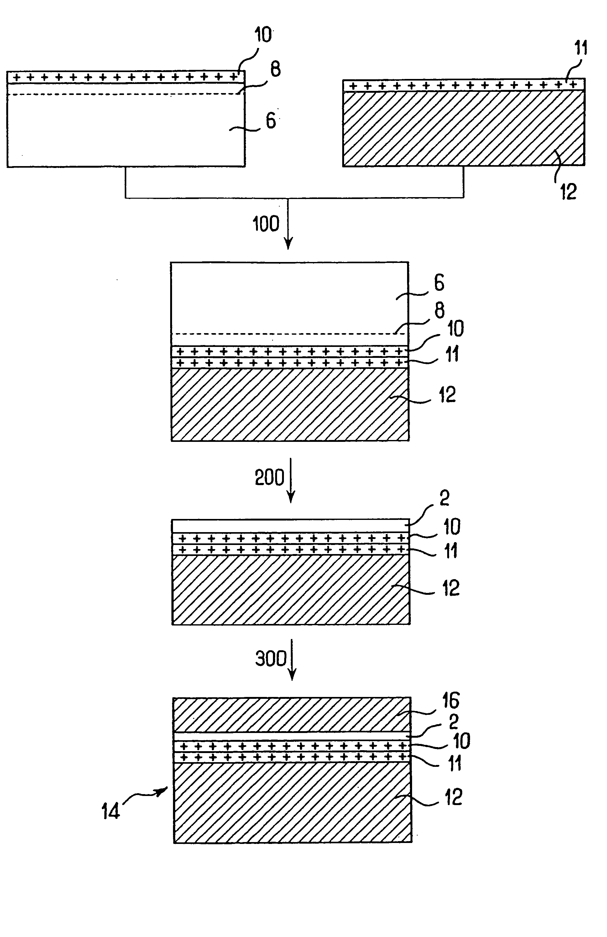
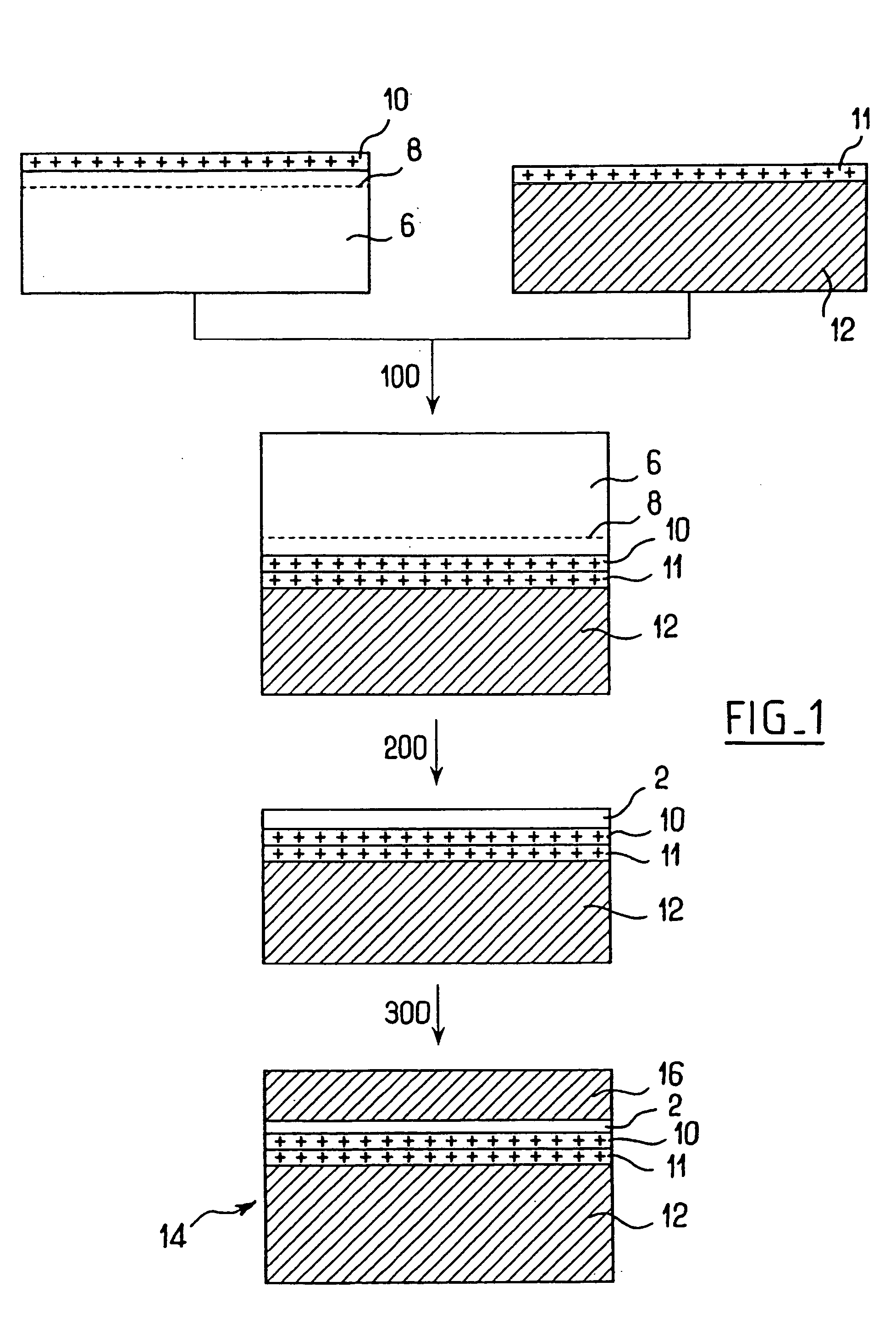
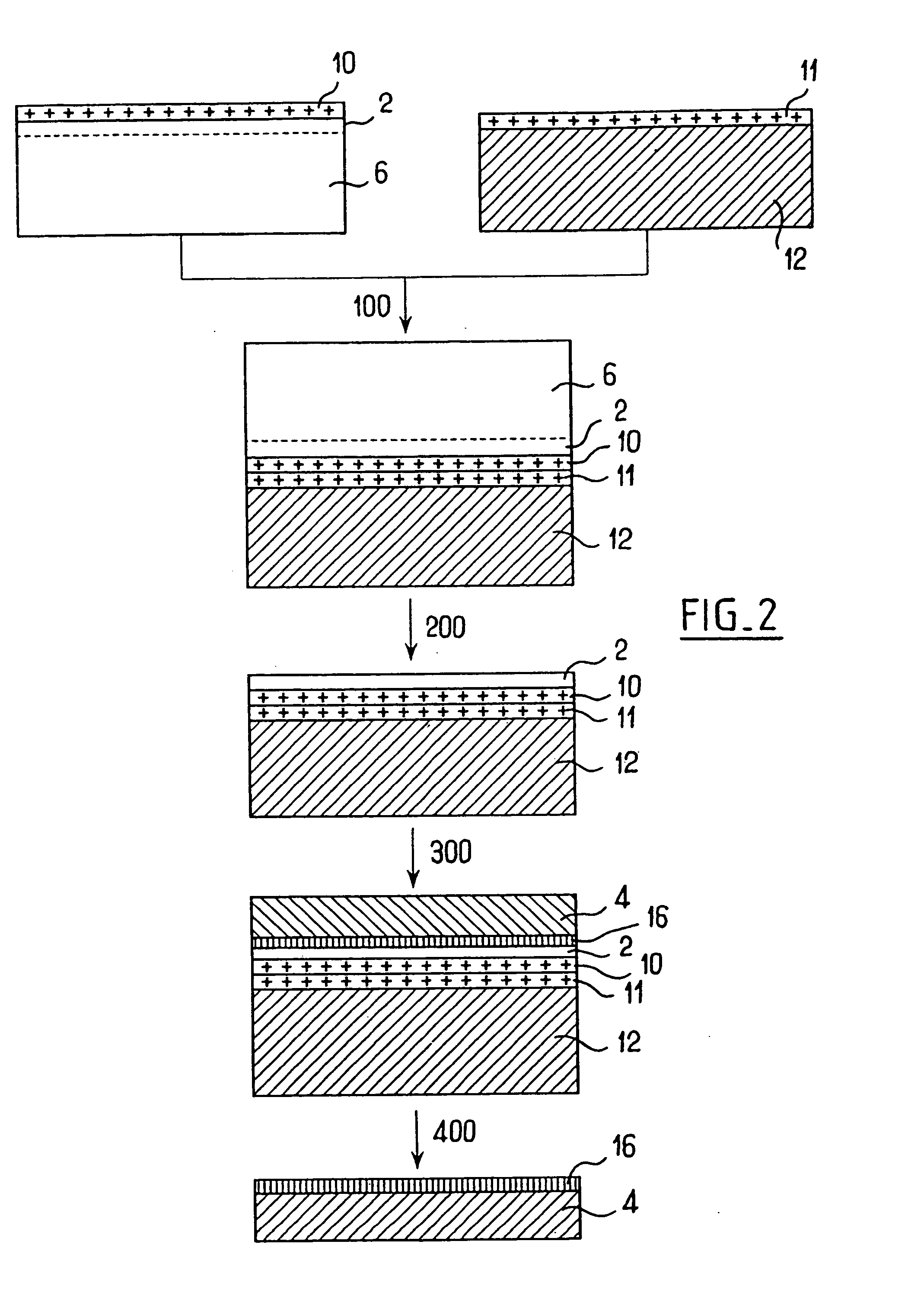
[0048] In the example corresponding to the first row of Table 2, a working layer 16 is made of gallium nitride on a seed layer 2 constituted by monocrystalline silicon carbide, itself on a polycrystalline silicon carbide support 12, with bonding layers 10 and 11 of silicon carbide being interposed between the support 12 and the seed layer 2. By way of example, the seed layer 2 is 1000 Å thick. The support 12 is 300 μm thick, for example.

[0049] The structure comprising a stack of the seed layer 2 of monocrystalline silicon carbide, the two bonding layers 10 and 11 of silicon oxide, and the support 12 of polycrystalline silicon carbide is made by a layer transfer method known to the person skilled in the art (e.g. see an application of the Smart-Cut® method in French patent No FR 2,681,472 or U.S. Pat. No. 5,374,564, each of which is expressly incorporated herein by reference thereto).

[0050] The working layer 16 can be made by chemical vapor deposition (CVD), by high temperature che...

example 2

[0052] In this example (second row of above table), a structure is provided that is equivalent to that of Example 1, except that the seed layer 2 of silicon carbide is replaced by a seed layer 2 of {111} silicon.

[0053] The thickness of the {111} silicon is preferably limited to less than 3000 Å so as to enable it to adapt without cracking to the thermal expansion that will take place during the various operations mentioned above.

example 3

[0054] In this example (third row of the above table), a structure is made that is equivalent to that of Examples 1 and 2, except that the seed layer 2 is made of sapphire.

[0055] Sapphire is another material that is known for permitting good epitaxy of gallium nitride.


PUM

PropertyMeasurementUnit
thicknessaaaaaaaaaa
thicknessaaaaaaaaaa
thicknessaaaaaaaaaa

Abstract

A method is provided for fabricating a substrate for optics, electronics, or opto-electronics. This method includes the steps of implanting atomic species into a face of a source substrate to form a weakened zone therein corresponding to the depth of penetration of the atomic species; transferring the seed layer on to a support substrate by bonding a face of the support substrate to the face of the source substrate and detaching the seed layer from the source substrate; depositing a working layer on the seed layer to form a composite substrate comprising the support substrate, seed layer and working layer; and detaching the seed layer and the working layer from the support substrate to form a substrate. Advantageously, the support substrate comprises a material having a thermal expansion value of about 0.7 to 3 times the coefficient value of the working layer, and the seed layer includes a crystal lattice parameter sufficient for the epitaxial growth of the working layer onto the seed layer such that the working layer has a dislocation concentration of less than about 107 / cm2.

Description

CROSS REFERENCE TO RELATED APPLICATIONS [0001] This application is a continuation of application Ser. No. 10 / 446,605 filed May 27, 2003, which is a continuation of International Application PCT / FR01 / 03714 filed Nov. 26, 2000, the entire content of each of which is expressly incorporated herein by reference thereto.FIELD OF THE INVENTION [0002] The invention relates to methods for fabricating substrates, in particular for optics, electronics, or optoelectronics, and also to substrates obtained by such methods. More particularly, the substrates are also suitable for use in fabricating light-emitting and laser diodes. BACKGROUND OF THE INVENTION [0003] In the technology field of optics, electronics, and optoelectronics, it is often desirable to obtain substrates that comprise a working layer. Two types of methods are currently known for making such substrates. One method includes transferring a working layer from a source substrate onto a support substrate. The other method includes de...

Claims


Application Information

Patent Timeline
Patent Type & Authority Applications(United States)
IPC IPC(8): C30B25/02C30B25/18H01L21/04H01L21/762H01L33/48
CPCC30B25/02C30B25/18C30B29/403H01L29/1608H01L21/0445H01L21/76254C30B29/406H01L21/34
Inventor LETERTRE, FABRICEGHYSELEN, BRUNO
Owner SOITEC SA
Why Eureka
Try Eureka