Method for fabricating semiconductor device and display device

a technology of display device and semiconductor, applied in the direction of liquid/solution decomposition chemical coating, superimposed coating process, instruments, etc., can solve the problems of increasing cost, reducing yield, and inability to meet users' needs, so as to reduce defects and reduce unevenness.

Inactive Publication Date: 2005-02-03
SEMICON ENERGY LAB CO LTD
View PDF5 Cites 33 Cited by
  • Summary
  • Abstract
  • Description
  • Claims
  • Application Information

AI Technical Summary

Benefits of technology

[0014] In view of the above problems, it is an object of the present invention to alleviate unevenness due to the contact hole 102 for forming a contact with the conductive film 100 in the l...

Problems solved by technology

How to produce advanced electronic devices without increasing the cost becomes key; however, if reliability and quality are sacrificed, it is impossible to satisfy users' needs.
Defects in the devices using semiconductor elements are some of the factors to cause lower yield.
When forming a conductive film used for a wiring, disconnection and high resistivity of the wiring is occasionally caused by poor coverage of the conductive film.
The poor coverage mostly occurs around an opening where the conductive film makes a contact with the lower layer.
Further, the poor coverage can occur, for example, when the contact is not made since the opening is not covered with a wiring material, or when a part of a wiring becomes too thin.
Display defects and unevenness are often due to une...

Method used


Image

  • Method for fabricating semiconductor device and display device
  • Method for fabricating semiconductor device and display device
  • Method for fabricating semiconductor device and display device

Examples


embodiment 1

[0088] [Embodiment 1]

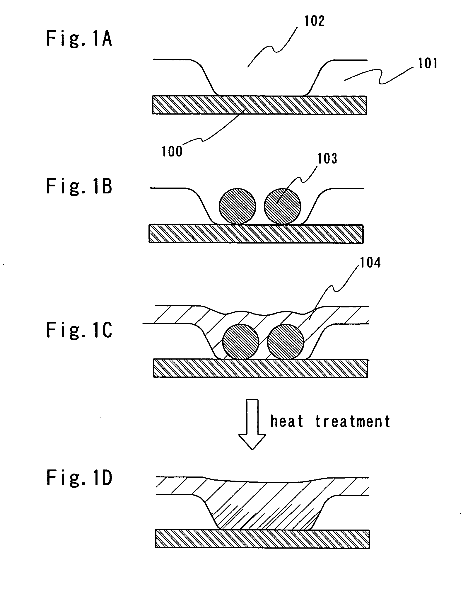
[0089] A fabrication method of an active matrix liquid crystal display device will be described as an example of the invention with reference to FIGS. 11A to 11D and 12A to 12D. In this embodiment, a fabrication method of a semiconductor device using droplet discharging method is applied; however, the invention can be naturally applied to a conventional process employing photolithography.

[0090] Here a fabrication process of an active matrix liquid crystal display device in which an n-channel TFT (for switching) and a capacitor are formed over one substrate employing the invention will be described.

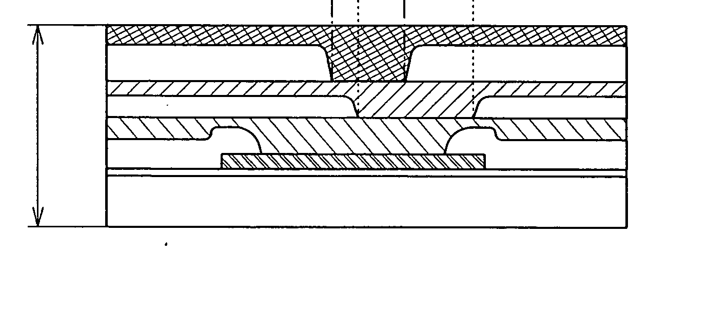
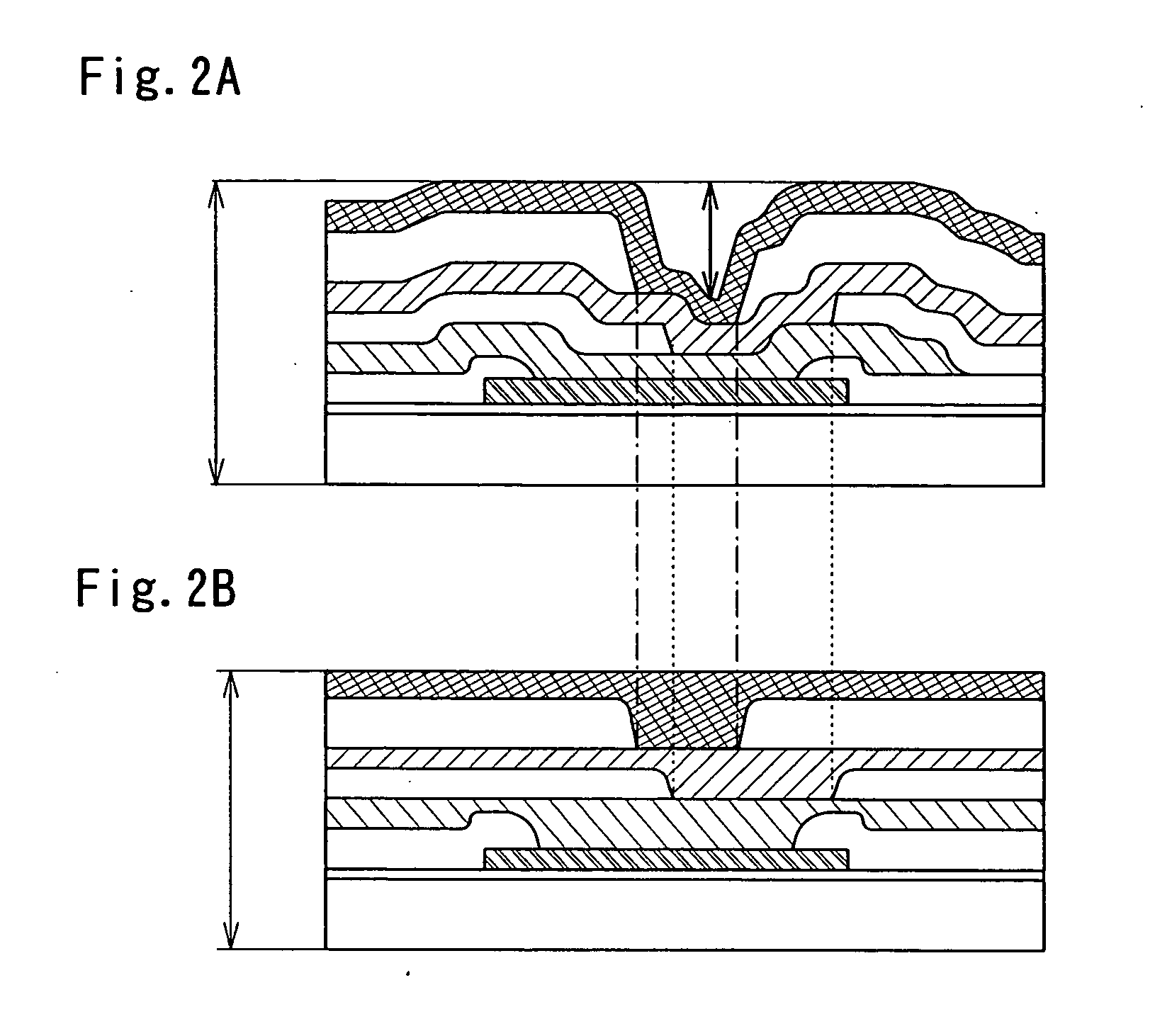
[0091] A substrate which withstands the process temperature of the process, such as a glass substrate or a flexible substrate typified by a plastic substrate is used for a substrate 601 (FIG. 11A). Specifically an active matrix substrate is made with a light transmitting substrate 601. The substrate with a large area as 600 mm×720 mm, 680 mm×880 mm, 1000 mm×1200 mm, ...

embodiment 2

[0120] [Embodiment 2]

[0121] Embodiment 2 of the invention will be described in more detail with reference to FIGS. 14A to 14E and FIGS. 15A to 15D. In this embodiment, a liquid crystal display device is partly used in a process for fabricating a semiconductor device; however, the invention can be naturally applied to a process using photolithography. The use or disuse of the conventional process is entrusted to those who employ the invention.

[0122] A glass substrate, a flexible substrate typified by a plastic substrate, or the like, which can withstand the processing temperature of the steps, is used for a substrate 801 (FIG. 15A). In this embodiment, the substrate 801 is made of glass. A base film 802 made of an insulating film is formed over the substrate 801. The base film 802 may have either a single layer structure or a layered structure. In this embodiment, the base film has a bilayer structure. A 50 nm thick silicon nitride oxide film is formed for the first layer and a 50 n...

embodiment 3

[0144] [Embodiment 3]

[0145] In this embodiment, an example of applying the invention to a bottom gate TFT of a channel etch type, will be described with reference to FIGS. 16A to 16D.

[0146] A gate electrode 610 is formed of Ta, Cr, Mo, Al or the like over a substrate 600. A gate insulating film 601 is formed of a silicon nitride film, a silicon oxide film, a tantalum oxide film, or the like over the substrate 600. A semiconductor film 602 having an amorphous structure is formed thereon so as to partially overlap with the gate electrode 610. The semiconductor film 602 having the amorphous structure is typically formed of amorphous silicon to a thickness of from 100 nm to 250 nm by plasma CVD. A semiconductor layer provided with n-type or p-type conductivity is formed so as to overlap the semiconductor film 602 having an amorphous structure. The semiconductor film 602 having an amorphous structure and the semiconductor layer are processed into island films, and then a film made of Cr...


PUM

PropertyMeasurementUnit
Electrical conductoraaaaaaaaaa
Areaaaaaaaaaaa

Abstract

It is an object of the present invention to alleviate unevenness due to an opening for making a contact with the lower layer even when the opening has a large diameter (1 μm or more). Thus, it is a further object of the invention to reduce defects caused by the unevenness due to the contact hole. It is a feature of the invention to form a wiring by filling the contact hole with conductive fine particles. The conductive fine particles can be easily dispersed into a wiring material by using conductive fine particles having high wettability with the wiring material, thereby making a contact. Thus, planarization of a contact hole can be achieved without performing a reflow process. Further, more planarity can be obtained by performing a reflow process in addition, and the reliability is improved accordingly.

Description

BACKGROUND OF THE INVENTION [0001] 1. Field of the Invention [0002] The present invention relates to a method for fabricating a semiconductor device. More specifically, the invention relates to a method for forming a contact between wirings of a semiconductor device. [0003] 2. Description of the Related Art [0004] In recent years, in accordance with the development of technology, miniaturization and performance of electronic devices has been advanced, and the highly developed electronic devices are everywhere. In order to maintain a company's competitive edge, it has become very important not only to produce better products than other companies, but also to offer such products at lower prices. [0005] How to produce advanced electronic devices without increasing the cost becomes key; however, if reliability and quality are sacrificed, it is impossible to satisfy users' needs. Higher production yields is a very effective measure to achieve further price reduction without degrading per...

Claims


Application Information

Patent Timeline
IPC IPC(8): G02F1/1362H01L21/288H01L21/768H01L21/77H01L21/84
CPCG02F1/136227H01L21/288H01L27/1292H01L21/76877H01L21/76882H01L21/7684
Inventor YAMAZAKI, SHUNPEI
Owner SEMICON ENERGY LAB CO LTD
Why Eureka
Try Eureka