Organic EL device and preparation method

a technology of organic el and el foil, which is applied in the direction of discharge tube luminescnet screen, natural mineral layered products, transportation and packaging, etc., can solve the problems of limiting the construction of organic layers which can be formed as laminates, and reducing the efficiency of vacuum evaporation. , to achieve the effect of high efficiency, high reliability and ease of handling

Inactive Publication Date: 2005-03-24
FUTABA CORPORATION +1
View PDF3 Cites 31 Cited by
  • Summary
  • Abstract
  • Description
  • Claims
  • Application Information

AI Technical Summary

Benefits of technology

A first object of the invention is to provide an organic EL device having a multilayer structure of organic layers formed by coating, featuring a high efficiency, high reliability and ease of handling as well as a high luminance and a long lifetime; and a method for preparing an organic EL device having a high efficiency and high reliability which enables organic layers to be formed in a multilayer structure by coating, so that the device can be simply prepared within a short time.

Problems solved by technology

In organic EL devices, what becomes a problem in injecting electrons from a metallic cathode into an organic compound which is deemed to be substantially insulating is the energy barrier.
The vacuum evaporation technique, however, is not regarded efficient as the device fabrication process because it is difficult to form homogeneous, defect-free thin films and time consuming in depositing a plurality of organic layers.
However, these patents use organic layers of the single layer structure, and do not take into account organic layers of the multilayer structure capable of more efficient light emission.
In these multilayer structures, however, particularly when a common coating solvent is used, the construction of organic layers which can be formed as a laminate is restricted, and the compound which can be used in introducing a crosslinking structure is limited.
The functional groups which must be introduced into the light emitting layer for crosslinking serve to reduce the efficiency of light emission of the resulting organic EL devices.
In such electrodes, the electrode material can diffuse into the polymer to become a dopant or to quench luminescence, resulting in devices which are often short-lived in continuous driving.
The materials of the cathode electrode are limited to high-melting metals.
On the other hand, the finished PPV raises a problem with respect to uniformity and has the drawback that device characteristics are very poor as compared with the recently developed soluble PPV.
Since metallic Li having a considerably high reactivity is admixed, control of the atmosphere is very difficult.
In the case of coating which entails a combination of a solvent with a material, the material suited for the evaporation is not directly applicable.
When a metal having a low work function is used as the cathode, it is very unstable independent of the way of forming the organic layer.
However, it is still necessary to use metals having a low work function and salts thereof, which are cumbersome to handle during the manufacture.
Degradation of such metals is still a problem.

Method used


Image

  • Organic EL device and preparation method
  • Organic EL device and preparation method
  • Organic EL device and preparation method

Examples


first embodiment

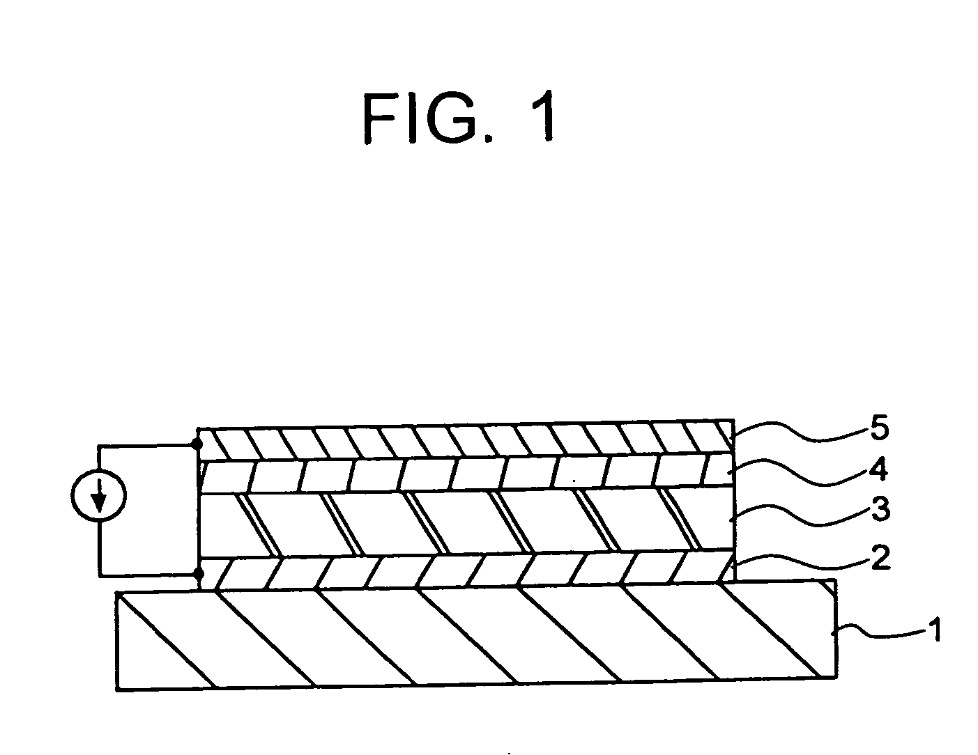
According to the first embodiment of the invention, the organic EL device has an anode 2 on a substrate 1 as shown in FIG. 1. Stacked on the anode 2 are an organic layer 3, typically a light emitting layer, an electron injecting layer 4, and a cathode 5. The organic layer 3 may be a single layer or consist of a plurality of layers. The order of stacking may be reversed. The stack construction may be any appropriate one depending on a particular display specification and manufacture process.

The electron injecting layer 4 close to the cathode 5 is an electron injecting organic layer containing an organic metal salt and / or organic metal complex of a metal having a standard electrode potential of more negative than −1.8 V at 25° C., and formed by coating. In this embodiment, an organic polymer layer containing a high molecular weight EL material is disposed close to the electron injecting organic layer.

The provision of such an electron injecting organic layer ensures a high electro...

embodiment (

ii) Having an Electron Injecting Layer Containing an Inorganic Metal Salt and / or Organic Metal Salt of a Metal Having a Standard Electrode Potential from −1.8 V to −0.8 V at 25° C.

The metals of the inorganic and organic metal salts should have a standard electrode potential at 25° C. between −1.8 V and −0.8 V, and preferably between −1.7 V and −1.15 V. The metals should preferably have a work function of at least 4.0 eV, but generally up to about 6 eV.

Examples of suitable metals include Al (III), Mn (II), Zr (IV), Ti (II), Hf (IV), Ta (V), Nb (III) and V (II). Preferred metals are Al (III), Mn (II) and Zr (IV), with Al (III) and Mn (II) being more preferred. Al (III) is most preferred.

As used herein, the inorganic metal salts include inorganic acids whose hydrogen is substituted with a metal, for example, metal halides such as chlorides, fluorides, bromides and iodides.

The organic metal salts include organic acids, alcohols and dialkylamides whose hydrogen is substituted with...

second embodiment

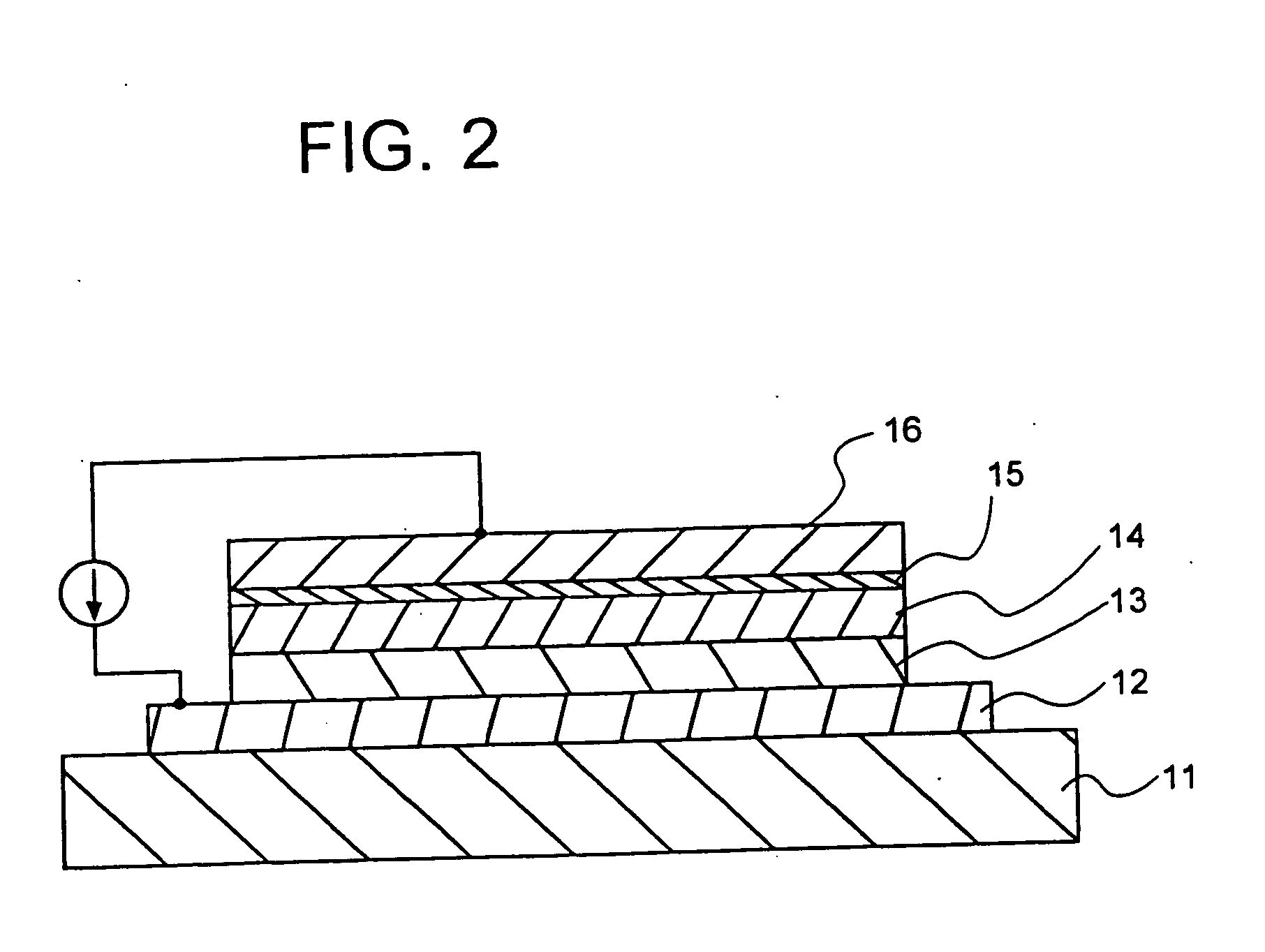
The organic EL device according to the second embodiment of the invention has, in order, a substrate, a first electrode on the substrate, two or more stacked organic layers on the first electrode including a light emitting layer, and a second electrode on the organic layers. At least one layer of the two or more stacked organic layers other than the light emitting layer contains at least one high or low molecular weight compound selected from among oxadiazole, triazole, thiadiazole, quinoline, quinoxaline, phenanthroline, and derivatives thereof. The light emitting layer contains a π-conjugated polymer, polyvinyl compound, polyacrylate, polymethacrylate or a derivative thereof. These organic layers are formed by coating.

Light emission takes place at a very high efficiency when the light emitting layer contains at least one of π-conjugated polymers, polyvinyl compounds, polyacrylate, polymethacrylate and derivatives thereof, and at least one organic layer other than the light emit...


PUM

PropertyMeasurementUnit
work functionaaaaaaaaaa
standard electrode potentialaaaaaaaaaa

Abstract

In an organic EL device comprising a cathode, an anode, and two or more stacked organic layers therebetween including a light emitting layer, an electron injecting organic layer containing an organic salt or complex of a metal having a standard electrode potential of more negative than −1.8 V at 25° C. is formed close to the cathode by coating, and an organic layer containing a high molecular weight EL material is disposed close to the electron injecting organic layer. A multilayer structure of organic layers can be formed by coating, and the organic EL device has a high luminance, high efficiency, high reliability, long life and ease of handling.

Description

This invention relates to organic electroluminescent (EL) devices having organic layers formed and stacked by coating, and more particularly, organic EL devices having high reliability and efficiency. It also relates to a method for preparing organic EL devices using a coating solvent capable of forming a stable amorphous film without attacking any underlying layer. It further relates to organic EL devices using stable metal salts which have never been used as the cathode or electron injecting electrode in the art. BACKGROUND OF THE INVENTION Since the announcement by Kodak of multilayer structure organic EL devices using a vacuum evaporation technique, the development of organic EL displays has been a great concern and reached the verge of commercial application. In organic EL devices, what becomes a problem in injecting electrons from a metallic cathode into an organic compound which is deemed to be substantially insulating is the energy barrier. It is desired to reduce the ene...

Claims


Application Information

Patent Timeline
Patent Type & Authority Applications(United States)
IPC IPC(8): C09K11/06H05B33/20H01L51/00H01L51/30H01L51/50
CPCC09K11/06C09K2211/1011C09K2211/1014C09K2211/1029C09K2211/1044C09K2211/181Y10T428/24917H01L51/0039H01L51/005H01L51/0079H01L51/5012H01L51/5092Y10S428/917C09K2211/182Y10T428/31692Y10T428/31855H10K85/115H10K85/60H10K85/321H10K50/11H10K50/171H05B33/20
Inventor KAMBE, EMIKOSHINKAI, MASAHIRO
Owner FUTABA CORPORATION
Why Eureka
Try Eureka