

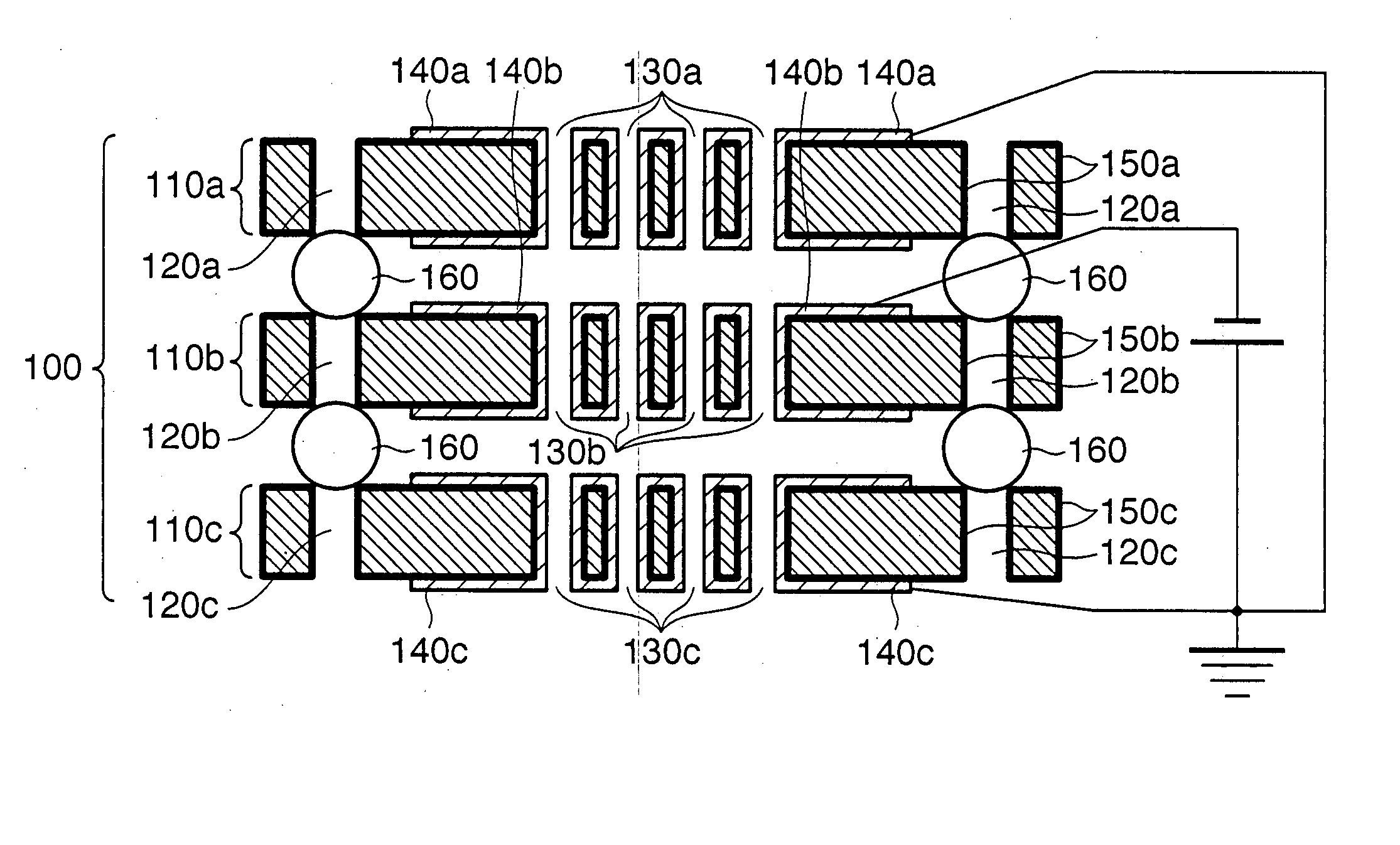
Multi-charged beam lens and charged beam exposure apparatus using the same
a charge-beam exposure and lens technology, applied in the direction of photomechanical equipment, instruments, beam deviation/focusing by electric/magnetic means, etc., can solve the problems of generating electrons or secondary electron avalanches, reducing the operating voltage or operational reliability of the electron lens, etc., to achieve high performance and reliability, and more resistant to surface discharge
- Summary
- Abstract
- Description
- Claims
- Application Information
AI Technical Summary
Benefits of technology
Problems solved by technology
Method used
Image

Examples
application example
Device Manufacturing Method
[0069] An application example of a device manufacturing method using the above-mentioned electron beam exposure apparatus will be described next.
[0070]FIG. 9 shows the manufacturing flow of a microdevice (e.g., a semiconductor chip such as an IC or LSI, liquid crystal panel, CCD, thin-film magnetic head, micromachine, or the like). In step 1 (circuit design), a semiconductor device circuit is designed. In step 2 (EB data conversion), the exposure control data for an exposure apparatus is created on the basis of the designed circuit pattern. In step 3 (wafer manufacture), a wafer is manufactured by using a material such as silicon. In step 4 (wafer process) called a preprocess, an actual circuit is formed on the wafer by lithography using the wafer and the exposure apparatus into which the prepared exposure control data is input. Step 5 (assembly) called a post-process is the step of forming a semiconductor chip by using the wafer formed in step 4, and in...
PUM
 Abstract
Description
Claims
Application Information