Thin film capacitor, thin film capacitor array and electronic component

a thin film capacitor and array technology, applied in the direction of fixed capacitors, fixed capacitor details, instruments, etc., can solve the problems of poor characteristics, degraded reliability, cracking of films, etc., and achieve the effect of shortening the distance, reducing electrode resistance, and reducing current paths

Active Publication Date: 2005-04-28
KYOCERA CORP
View PDF7 Cites 4 Cited by
  • Summary
  • Abstract
  • Description
  • Claims
  • Application Information

AI Technical Summary

Benefits of technology

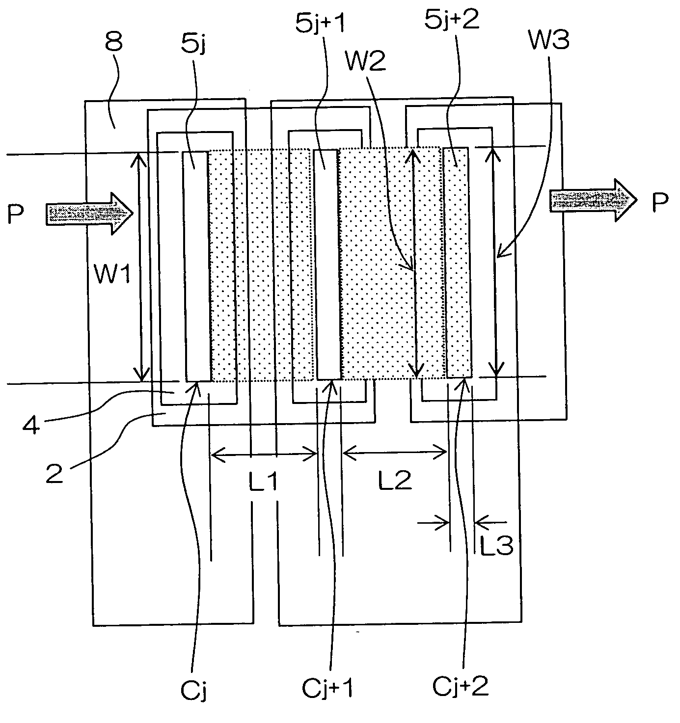
[0018] (3) a distance L3 of one of the upper electrode formed on the lower electrode along a high frequency signal propagation direction is smaller than a length W3 along the direction perpendicular to the high frequency signal propagation direction at an area where the upper electrodes and the extraction electrode overlap in plan view. By employing any of the aforementioned constructions (1)-(3), in comparison to thin film capacitors with the same number of capacitance elements that do not employ any of the constructions (1)-(3), the distance between the input terminal and output terminal can be shortened, so that a miniaturized thin film capacitor that enables high density packaging can be produced. In addition, since the resistance of the electrodes connecting the capacitance elements to each other can be reduced, insertion loss of the thin film capacitor can be reduced, so that the Q-value thereof can be increased.
[0036] In any of the constructions described above, it is preferable that the thin film dielectric be formed using (Bax, Sr1-x)yTi1-yO3-x. This makes it possible to produce a variable-capacitance capacitor having variable-capacitance elements with large capacitance change and minimal loss. Here, 0<x<1, 0<y<1, and z is slightly greater than 0 and considerably less than 1.

Problems solved by technology

However, as the number of layers increases, besides problems such as misalignment in the photolithography process and damage to the lower layers during etching, stress is enhanced by the increase in number of the layers, resulting in cracking in the films, which leads to poor characteristics and degraded reliability.

Method used


Image

  • Thin film capacitor, thin film capacitor array and electronic component
  • Thin film capacitor, thin film capacitor array and electronic component
  • Thin film capacitor, thin film capacitor array and electronic component

Examples


example

[0102] An example will be given for describing the present invention more specifically.

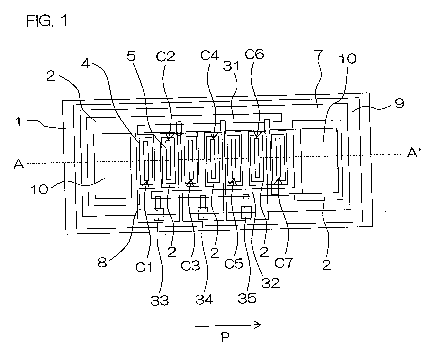
[0103] First, a sapphire R substrate was used as the supporting substrate 1. Pt was used as the material for the lower electrodes 2 and deposited on the supporting substrate 1 by sputtering at a substrate temperature of about 500° C. Before initiating the deposition of the thin film dielectrics 4, annealing for flattening the lower electrodes 2 formed of Pt was carried out by keeping the sample at about 800° C. The deposition of the thin film dielectrics 4 was carried out using (Ba0.5Sr0.5) TiO3 as the target at a substrate temperature of about 800° C. for 15 minutes. The upper electrodes 5 each consisting of two layers including a Pt electrode layer as the lower layer and a Au electrode layer as the upper layer were deposited on the thin film dielectrics 4. The above described deposition processes were successively carried out within the same chamber without exposing to the atmospheric air.

[010...


PUM


Abstract

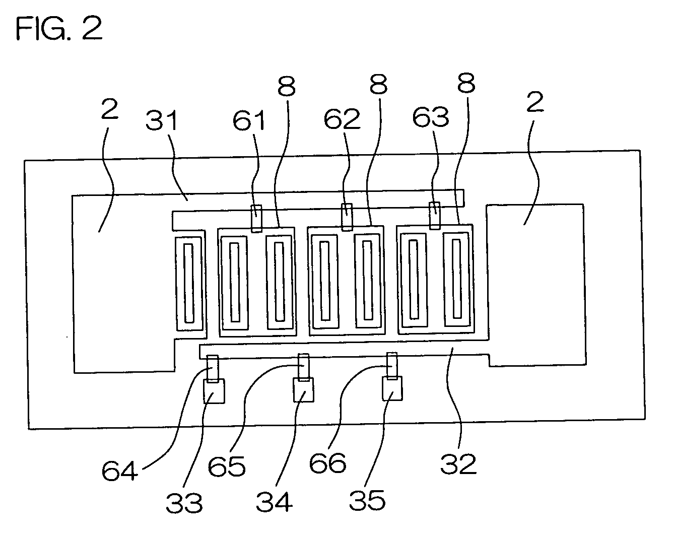
A thin film capacitor with small electrode resistance and great Q-value which comprises a small number of thin films that are deposited successively is disclosed. It is effective for miniaturization and high density packaging of a device and for preventing poor characteristics and degradation of reliability. A plurality of lower electrodes 2 are provided on a supporting substrate 1, which are spaced apart from each other in a high frequency signal propagation direction P. Two upper electrodes 5 spaced apart from each other in the high frequency signal propagation direction P are provided on one of the plurality of the lower electrodes 2 through a thin film dielectric layer 4, by which two capacitance elements are formed. The upper electrodes 5 are connected together by an extraction electrode 8 so that the two capacitance elements are connected in series. A maximum distance L1 between the two upper electrodes 5 in the high frequency signal propagation direction P is smaller than a minimum length W1 of the upper electrodes 5 in the direction perpendicular to the high frequency signal propagation direction P in plan view.

Description

BACKGROUND OF THE INVENTION [0001] 1. Field of the Invention [0002] The present invention relates to a thin film capacitor, capacitor array comprising a plurality of the thin film capacitors connected in parallel to one another, and an electronic component using these. The electronic component is represented particularly by voltage controlled high frequency resonator, voltage controlled high frequency filter, voltage controlled matching circuit chip, voltage controlled antenna duplexer and the like with excellent power handling capability. [0003] 2. Description of Related Art [0004] There is a conventionally known thin film capacitor comprising a supporting substrate with electrical insulation, a thin film lower electrode, a thin film dielectric layer and a thin film upper electrode layer successively stacked in this order. In such a thin film capacitor, the lower electrode layer and upper electrode layer are deposited by sputtering, vacuum deposition or the like, and the thin film ...

Claims


Application Information

Patent Timeline
IPC IPC(8): H01G4/33H01G7/06H01L21/00H01L27/01
CPCH01L27/016H01G4/33
Inventor KUSABE, KAZUHIRO
Owner KYOCERA CORP
Why Eureka
Try Eureka