Porous silicon composite structure as large filtration array
- Summary
- Abstract
- Description
- Claims
- Application Information
AI Technical Summary
Benefits of technology
Problems solved by technology
Method used
Image
Examples
Embodiment Construction
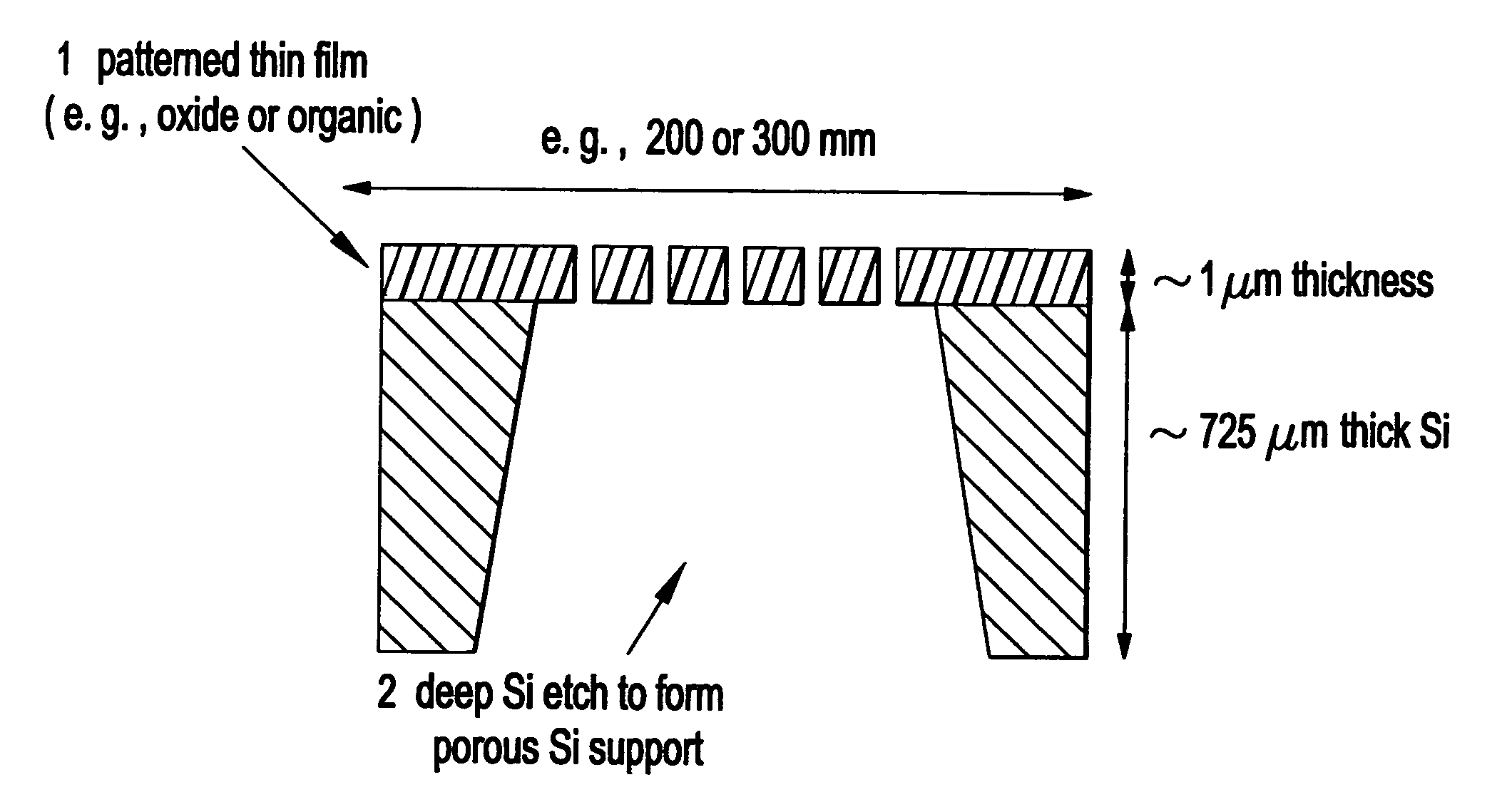
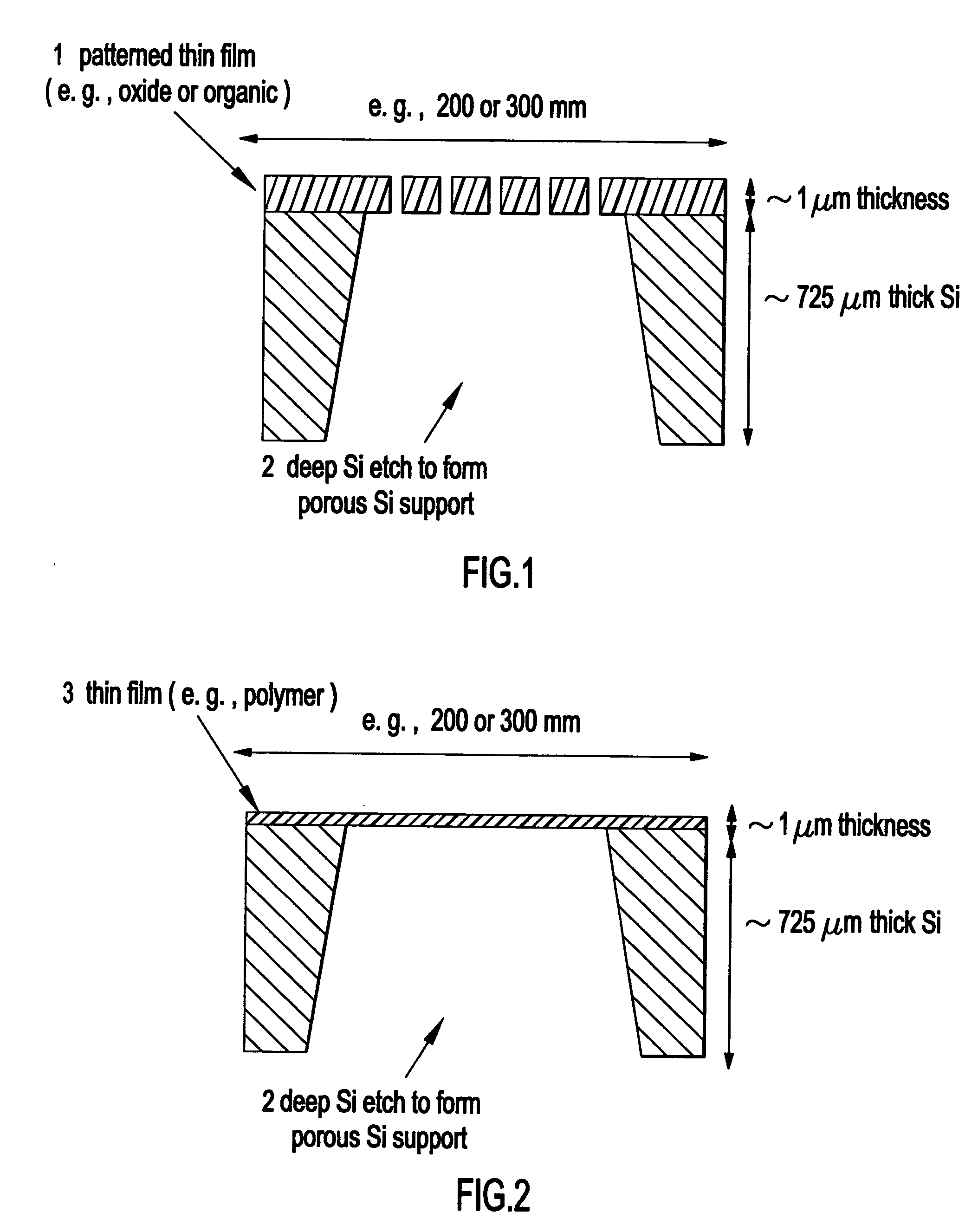
[0021] The filter membrane structure shown in FIG. 1 uses a thin separation layer 1, which can be an inorganic, for example SiO2, or an organic material, that is lithographically patterned by a method known in the art to form a channel-pore structure. A channel-pore structure permits a size-selective process in which molecules larger than the diameter of the channel-pores are retained, while the smaller molecules elute. The thin separation layer 1 is deposited on a bulk crystalline silicon support membrane 2. Spin glass, such as siloxanes, silsesquioxanes, N-silsesquioxanes, and polycabosilanes also can be used to form a separation layer, as can polyimide, polysulfone, and polyethersulfone.
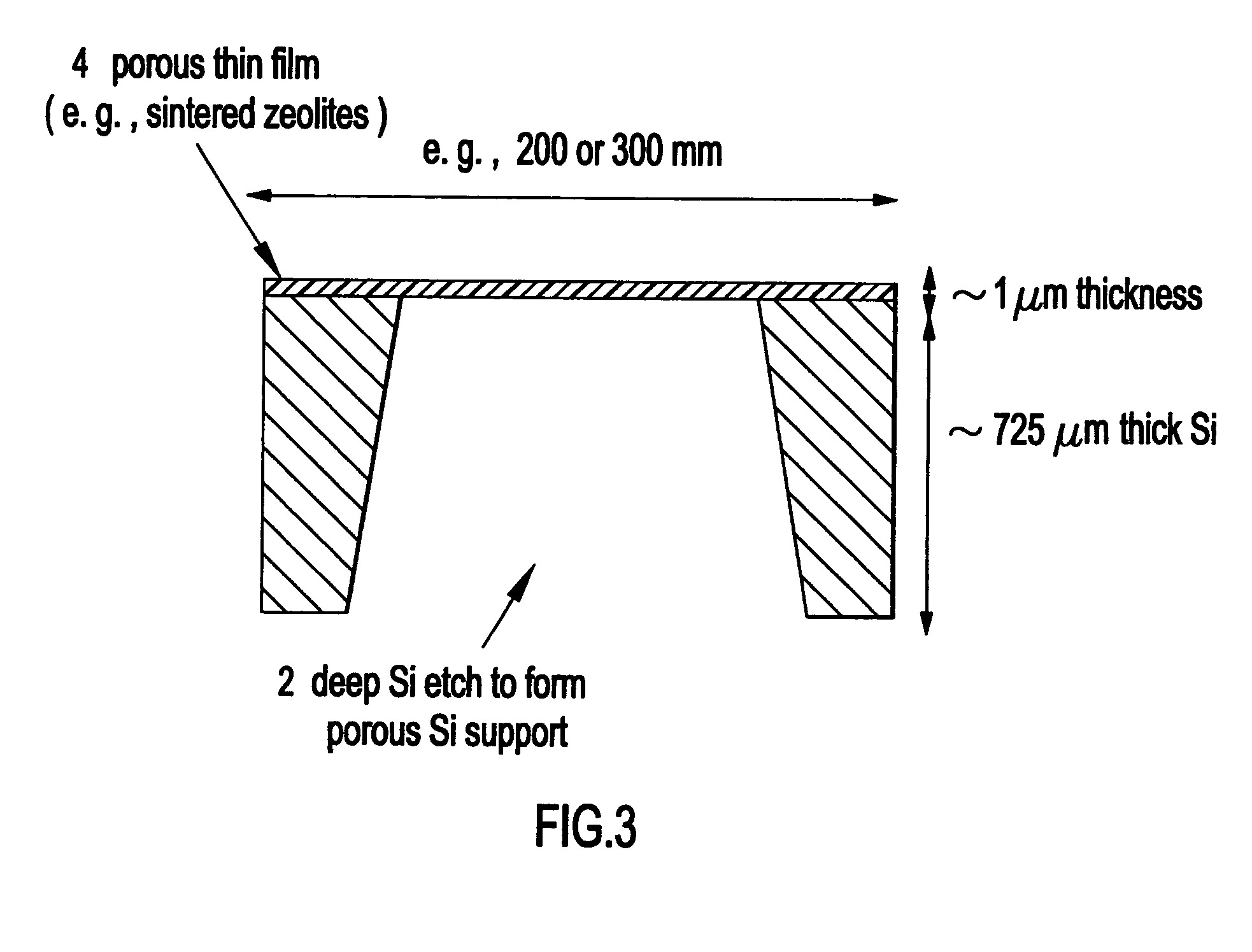
[0022] The silicon material comprises a wafer thickness which, as manufactured, is between about 725 and about 750 μm notmm thick. Thin film separation layer 2 can be deposited by a number of methods known to those skilled in the art, such as chemical vapor deposition (CVD), plasma-enhanced CVD, ...
PUM
| Property | Measurement | Unit |
|---|---|---|
| Thickness | aaaaa | aaaaa |
| Diameter | aaaaa | aaaaa |
| Structure | aaaaa | aaaaa |
Abstract
Description
Claims
Application Information


