

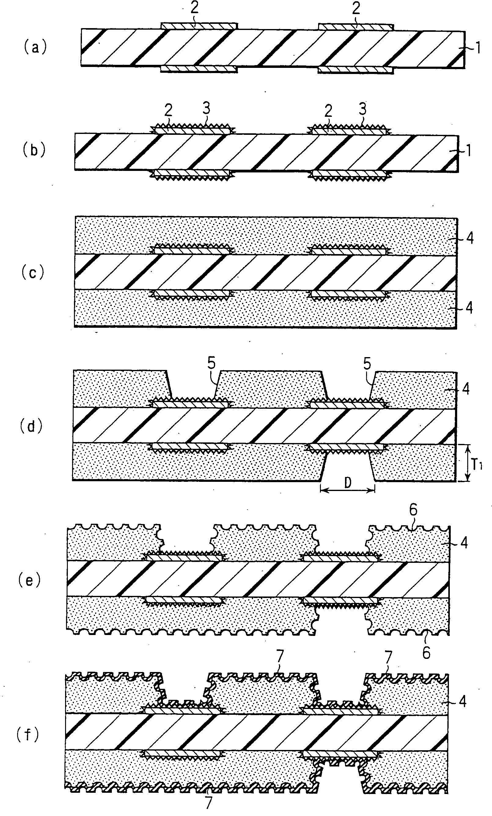
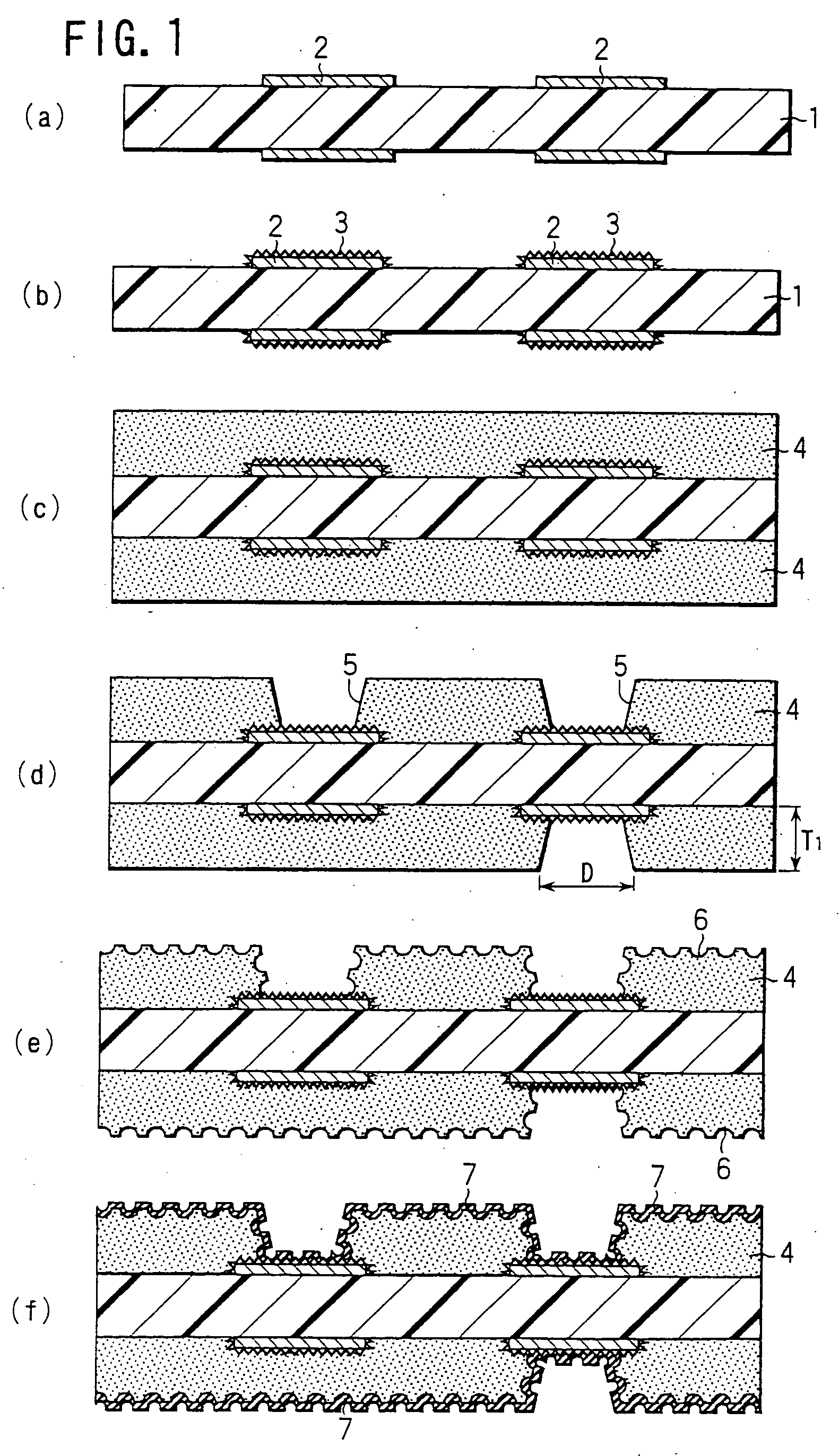
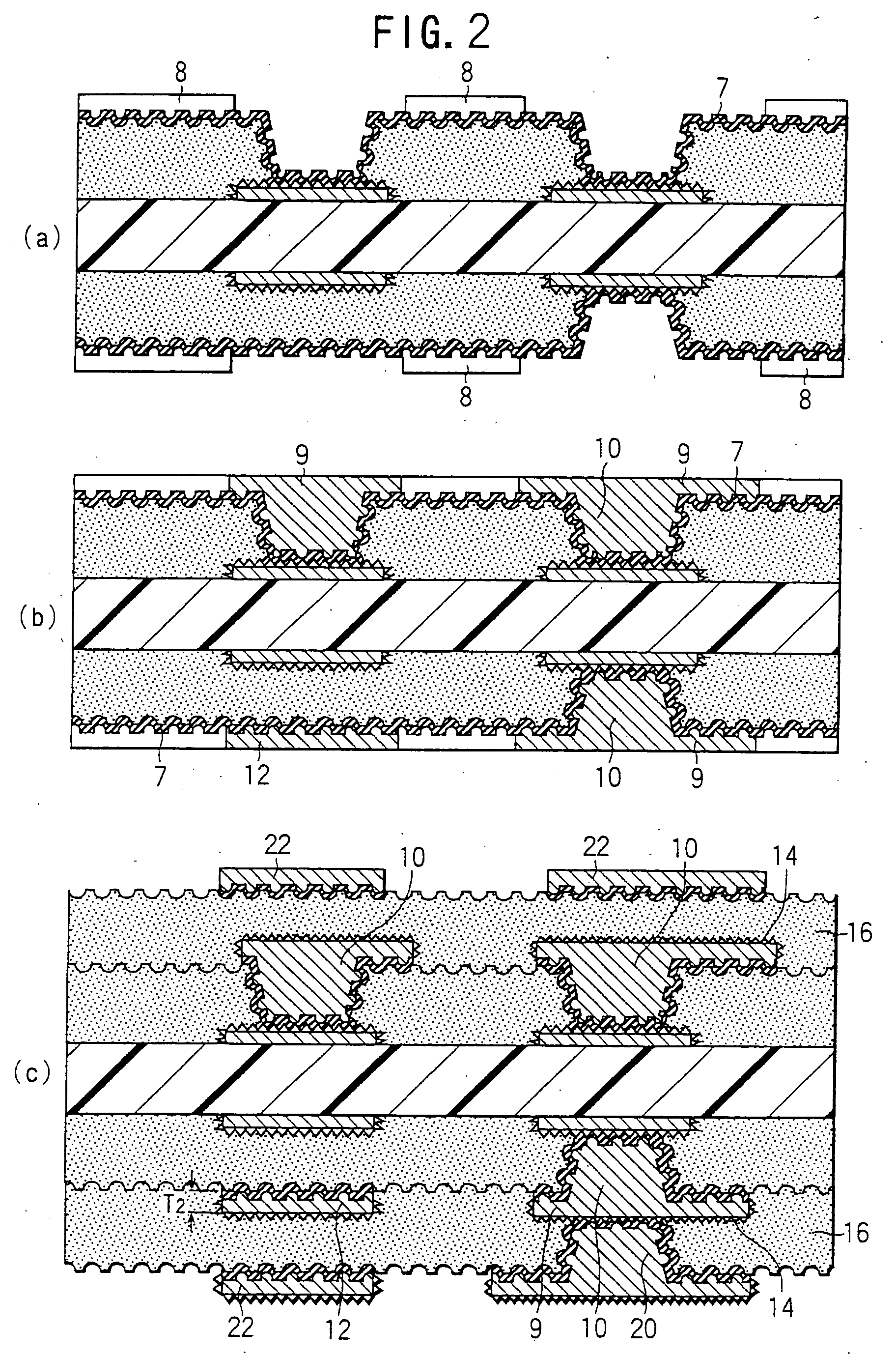
Multilayer printed wiring board with filled viahole structure
a printing board and viahole technology, applied in the direction of printed element electric connection formation, dielectric characteristics, conductive pattern formation, etc., can solve the problems of metal deposit likely to break, surface portion of plating metal exposed outside the hole for viahole, etc., to achieve improved adhesion between the viahole and the interlaminar insulative resin layer, the effect of large malleability and strong adhesion
- Summary
- Abstract
- Description
- Claims
- Application Information
AI Technical Summary
Benefits of technology
Problems solved by technology
Method used
Image

Examples
example 1
[0170] (1) Compositions prepared through the following steps {circle over (1)} to {circle over (3)} were mixed together and agitated to prepare an electroless plating adhesive.
[0171] {circle over (1)} Thirty-five parts by weight of a 25% acrylated product of cresol novolac type epoxy resin (80% in sold content; 250 in molecular weight, by Nippon Kayaku Co., Ltd.), 4 parts by weight of photosensitive monomer (ARONIX M315 by Toa Gosei Co., Ltd.), 0.5 part by weight of antifoaming agent (S-65 by SANNOPCO) and 3.6 parts by weight of NMP, were mixed by agitation.
[0172] {circle over (2)} Eight parts by weight of polyether sulfone (PES) and 7.245 parts by weight of epoxy resin particles (POLYMERPOE by Sanyo Kasei Co., Ltd.) of 0.5 μm in mean particle size were mixed together and then 20 parts by weight of NMP were added to the mixture. They were mixed by agitation.
[0173] {circle over (3)} Two parts by weight of imidazole curing agent (2E4MZ-CN by Shikoku Kasei Co., Ltd.), 2 parts by wei...
example 2
[0183] A multilayer printed wiring board was prepared in the same manner as the aforementioned example 1 except that an interlaminar insulative resin layer was formed by attaching a fluororesin film of 20 μm in thickness to the layer by thermo-compression bonding and holes for viaholes of 60 μm in diameter were formed by irradiating ultraviolet laser.
example 3
[0184] (1) A drawn tetrafluoroethylene resin (PTFE) fiber available as fiber for woven fabric from the W. L. Gore & Associates, Inc. (trade-name: GORE-TEX) was used to weave a cloth for an interlaminar insulative resin layer. The cloth was composed of 53 fibers of 400 deniers per 2.54 cm in longitudinal direction and 52 fibers of 400 deniers per 2.54 cm in lateral direction.
[0185] (2) The fluororesin fiber cloth was cut to a sheet of 15.24 cm by 15.24 cm, and the cloth sheet was immersed in a solution of alkaline metal and naphthalene available under the trade name TETRA-ETCH from the W. L. Gore & Associates. After that, the cloth sheet was washed in warm water to rinse away the acetone. The fibers appeared dark brown due to the etching and the cloth shrank 20% in both longitudinal and lateral directions. The cloth sheet was stretched to the initial dimensions with the edges thereof held in hands.
[0186] On the other hand, a liquid epoxy resin was prepared as a thermosetting resin ...
PUM
| Property | Measurement | Unit |
|---|---|---|
| diameter | aaaaa | aaaaa |
| thickness | aaaaa | aaaaa |
| thickness | aaaaa | aaaaa |
Abstract
Description
Claims
Application Information