Plasma etching method

a technology of etching and plasma, which is applied in the direction of chemistry apparatus and processes, electric discharge tubes, semiconductor devices, etc., can solve the problems of reducing yield in both cases, new problems may occur, and so as to reduce striation at etched portions, improve processing shape, and suppress the effect of widening an upper portion of a recess

Active Publication Date: 2005-05-12
TOKYO ELECTRON LTD
View PDF3 Cites 9 Cited by
  • Summary
  • Abstract
  • Description
  • Claims
  • Application Information

AI Technical Summary

Benefits of technology

[0008] Accordingly, the present invention strives to solve the problems occurring in case of etching, for example, an insulating film containing silicon and oxygen by using an active species generating gas including a compound having carbon and fluorine. It is, therefore, an object of the present invention to provide, in case of performing an etching on a substrate having a resist mask on which an interval between neighboring openings formed is set to be 200 nm or less, a plasma etching method capable of suppressing an undulation of inner peripheral s

Problems solved by technology

Meanwhile, with a recent trend for high integration of semiconductor devices, various problems have occurred.
In case the holes are closely located to such extent, however, a new problem may occur.
Given that the holes themselves are minute, various problems may be caused if the shapes of the holes become poor and irregular.
For instance, a desired capacitance cannot be obtained in case the holes are for use in burying capacitance devices, and an expected conductivity cannot be obtained in case the holes are formed as contact holes, resulting in a reduction of yields in both cases.
Further, if it is difficult to avoid cutting of angled portions of the resist mask 12 by an etching gas, and if resist portions between the holes 13 are very thin, the angled portions 14 may be cut at both sides, as shown in FIG. 15, and interferences therebetween may cause poor shapes of holes 13 which may be transferred to the holes of the SiO2 film, thereby reducing the yields.
For this reason, it is undesirable to have the selectivity reduced.
This problem also occurs for, e.g., a SiCOH film, which is receiving considerable attention as an interlayer insulating film with a low dielectric constant, as well as the SiO2

Method used


Image

  • Plasma etching method
  • Plasma etching method
  • Plasma etching method

Examples


example 1-1

B. EXAMPLE 1-1

[0066] Under the above processing conditions, the flow rates of Ar and Xe were set to be 1250 sccm and 150 sccm, respectively.

example 1-2

C. EXAMPLE 1-2

[0067] Under the above processing conditions, the flow rates of Ar and Xe were set to be 1150 sccm and 250 sccm, respectively.

example 1-3

D. EXAMPLE 1-3

[0068] Under the above processing conditions, the flow rates of Ar and Xe were set to be 1050 sccm and 350 sccm, respectively.

E. EXPERIMENTAL RESULTS

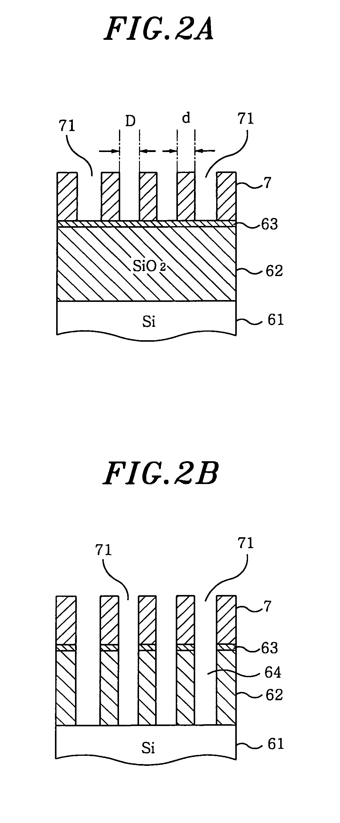
[0069] In each example, the shapes of holes 64 formed on the surface of the SiO2 film 62 were inspected through the use of a SEM (Scanning Electron Microscope) by removing the resist mask 7 after completing an etching of the SiO2 film 62, and a selectivity was obtained from the film thickness of the residual resist mask 7 and the depths of the holes 64 by way of halting the process in the middle of etching the SiO2 film. Further, the etching of the SiO2 film 62 was continued even after reaching a calculated end point, that is, an overetching was conducted.

[0070]FIG. 4 visualizes the experimental results, wherein the drawings are based on the pictures of top surfaces and cross sections obtained by the SEM. From the observation of the pictures, it can be found that the shapes of the holes 64 were poor in case of using the...


PUM


Abstract

A plasma etching is performed on a substrate having a pattern wherein an interval between neighboring openings formed on a resist mask is equal to or less than 200 nm, wherein the etching is performed by converting a processing gas comprising an active species generating gas which includes a compound having carbon and fluorine, and a nonreactive gas which includes xenon gas into a plasma. The nonreactive gas further includes argon gas.

Description

FIELD OF THE INVENTION [0001] The present invention relates to a plasma etching method for etching a surface of a substrate by using a gas composed of a compound containing carbon and fluorine. BACKGROUND OF THE INVENTION [0002] A manufacturing process of semiconductor devices may involve an etching process using a plasma, wherein the processing condition for the etching process, such as selection of the processing gas used, is determined based on the types of the film to be etched and the under film. For example, in order to etch a SiO2 film (silicon oxide film) or a SiCOH film (hydrogenated silicon oxycarbide film), which contains silicon and oxygen to serve as an insulating film, there has been known a method for converting a gas containing C (carbon) and F (fluorine) into a plasma to thereby allow SiO2 or SiCOH to be removed by a reaction with a CF based or a CHF based radical. For example, there has been known a method for performing an etching by using a CxFy gas (fluorocarbon...

Claims


Application Information

Patent Timeline
IPC IPC(8): H01L21/3065H01L21/311H01L21/28H01L21/768
CPCH01J37/32082H01L21/31138H01L21/31116
Inventor KATO, KAZUYAONO, KATSUHIKOMIZUNO, HIDEKIOGASAWARA, MASAHIROKITAMURA, AKINORIKOBAYASHI, NORIYUKIINATA, YASUSHIOKAMOTO, SHIN
Owner TOKYO ELECTRON LTD
Why Eureka
Try Eureka