Light emitting device and method of manufacturing the same

a technology of light emitting device and manufacturing method, which is applied in the manufacture of electric discharge tube/lamp, discharge tube luminescnet screen, electrode system, etc., can solve the problems of reducing affecting the light output so as to improve the light output efficiency of the light emitting element without deteriorating the characteristics of the anode material.

Inactive Publication Date: 2005-06-23
SEMICON ENERGY LAB CO LTD
View PDF31 Cites 10 Cited by
  • Summary
  • Abstract
  • Description
  • Claims
  • Application Information

AI Technical Summary

Benefits of technology

[0016] The present invention, in the manufacturing step of the light emitting element of the top emission, is to provide means of improving a l

Problems solved by technology

Therefore, backlight, which is used in conventional liquid crystal displays, is unnecessary.
However, in the bottom emission structure, even if resolution is tried to be raised, TFT and wiring may be interfered due to their arrangement.
Thus, a problem of a restriction of an apert

Method used


Image

  • Light emitting device and method of manufacturing the same
  • Light emitting device and method of manufacturing the same
  • Light emitting device and method of manufacturing the same

Examples


embodiment 1

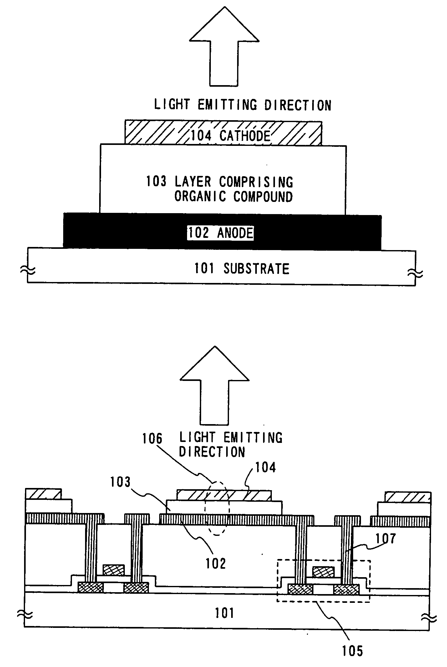
[0083] This embodiment gives a detailed description on the element structure of a light emitting element in a light emitting device of the present invention with reference to FIG. 4. Specifically, the element structure in which a low-molecular based compound is used for a layer comprising at least one organic compound will be described.

[0084] As described in Embodiment Mode, an anode 401 is formed from a light-shielding metal compound film. The anode 401 in this embodiment is an electrode electrically connected to a TFT 202 as in FIG. 3C, and is formed of TiN by sputtering to a thickness of 110 nm. Sputtering used here can be diode sputtering, ion beam sputtering, opposite target sputtering, or the like.

[0085] A layer comprising at least one organic compound 402 is formed on the anode 401. First, a hole injection layer 403 having a function of improving injection of holes from the anode is formed. The hole injection layer 403 in this embodiment is a copper phthalocyanine (Cu—Pc) f...

embodiment 2

[0099] In this embodiment, one of the element structures of light emitting devices of the present invention is described in detail with reference to FIG. 5. Especially, the element structure formed by using high-molecular compounds to the layer comprising at least one organic compound is described.

[0100] As mentioned in Embodiment Mode, an anode 501 is formed by the metal compound film having light blocking effect.

[0101] In this embodiment, the anode 501 is connected electrically to the TFT 202 as shown in FIG. 3C, and is formed by TaN to have a thickness of 110 nm using a sputtering method. As sputtering methods used in this embodiment, two polarity sputtering method, an ion beam sputtering method, an opposite target sputtering method, or the like.

[0102] In this embodiment, a layer comprising at least one organic compound 502 formed on the anode 501 has a lamination structure constituted a hole transporting layer 503 and a light emitting layer 504. Further, the layer comprising ...

embodiment 3

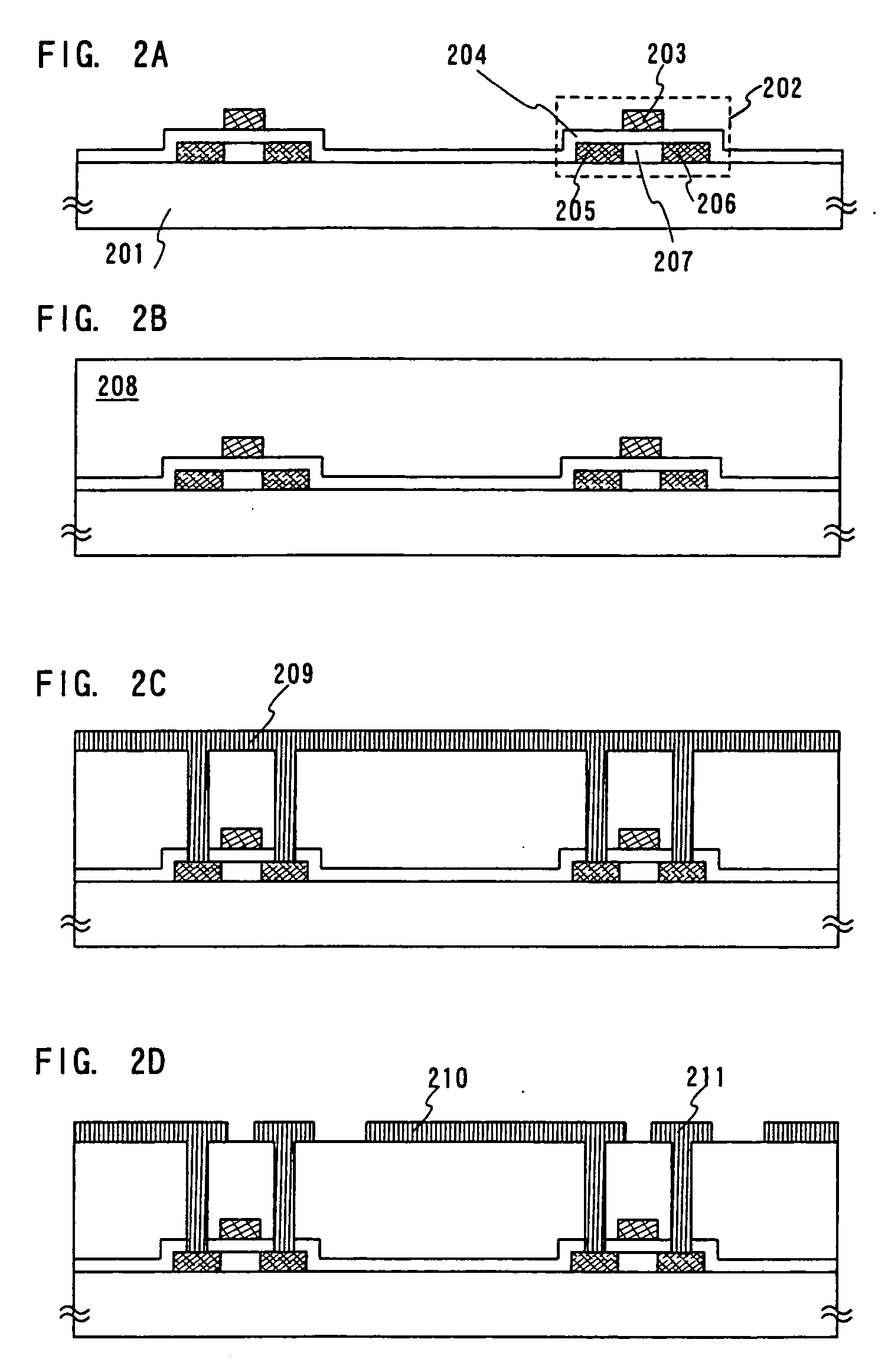
[0113] In forming a element substrate, a method of simultaneously forming, on the same substrate, a pixel portion and TFTs (n-channel TFT and p-channel TFT) of a driver circuit formed in the periphery of the pixel portion and forming a light emitting element which is electrically connected to the TFT at pixel portion are described in detail with reference to FIGS. 6 to 9 in this embodiment. Note that, in this embodiment, light emitting element having the structure described in Embodiment Mode is formed.

[0114] First, in this embodiment, a substrate 600 is used, which is made from glass, such as barium borosilicate glass or aluminum borosilicate, represented by such as Corning #7059 glass and #1737. Note that, as the substrate 600, there is not particular limitation if the substrate is transparent to the light, even a quartz substrate can be used. A plastic substrate having heat resistance to a process temperature of this embodiment may also be used.

[0115] Then, a base film 601 form...


PUM


Abstract

A measure for improving the light emission efficiency of a light emitting element without degrading characteristics of anode materials used in prior art is provided in manufacture of an upward emission type light emitting element. The present invention is characterized in that nitride or carbide of a metal element belonging to one of Group 4, 5, and 6 in the periodic table (hereinafter referred to as metal compound) is used as the material for forming an anode of a light emitting element. The metal compound has a work function equal to or larger than the work function of conventional anode materials. Therefore, injection of holes from the anode can be improved ever more. Also, with regard to conductivity, the metal compound is smaller in resistivity than ITO. It therefore can fulfil the function as a wire and can lower the drive voltage in the light emitting element compared to prior art.

Description

BACKGROUND OF THE INVENTION [0001] 1. Field of the Invention [0002] The present invention relates to a light emitting device using a light emitting element which has a layer containing an organic compound between a pair of electrodes and which can give fluorescence or luminescence by receiving an electric field. The light emitting device referred to in the present specification is an image display device, a light emitting device or a light source. Additionally, the following are included in examples of the light emitting device: a module wherein a connector, for example, a flexible printed circuit (FPC) or a tape automated bonding (TAB) tape, or a tape carrier package (TCP)) is set up onto a light emitting element; a module wherein a printed wiring board is set to the tip of a TAB tape or a TCP; and a module wherein integrated circuits (IC) are directly mounted on a light emitting element in a chip on glass (COG) manner. [0003] 2. Related Art [0004] A light emitting element is an el...

Claims


Application Information

Patent Timeline
IPC IPC(8): H01L27/32H01L51/50H05B33/26H01L51/52
CPCH01L27/3244H01L51/5096H01L2251/5315H01L51/5221H01L51/5284H01L51/5206H10K59/123H10K59/12H10K50/18H10K50/81H10K50/828H10K50/865H10K2102/3026H05B33/26
Inventor SEO, SATOSHINAKAMURA, YASUO
Owner SEMICON ENERGY LAB CO LTD
Why Eureka
Try Eureka