Semiconductor processing equipment having improved process drift control

a technology of process drift and processing equipment, applied in the direction of electrical equipment, chemical vapor deposition coating, coating, etc., can solve the problems of coating cracking, and achieve the effect of reducing particle contamination and/or process dri

a technology of process drift and processing equipment, applied in the direction of electrical equipment, chemical vapor deposition coating, coating, etc., can solve the problems of coating cracking, and achieve the effect of reducing particle contamination and/or process dri

US20050145176A1Inactive Publication Date: 2005-07-07LAM RES CORP

Image

  • Semiconductor processing equipment having improved process drift control
  • Semiconductor processing equipment having improved process drift control
  • Semiconductor processing equipment having improved process drift control

Examples


Embodiment Construction

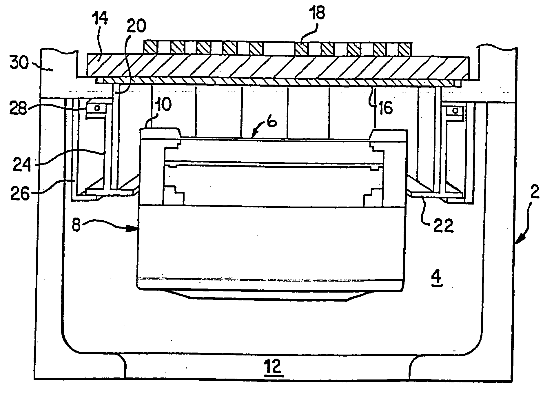
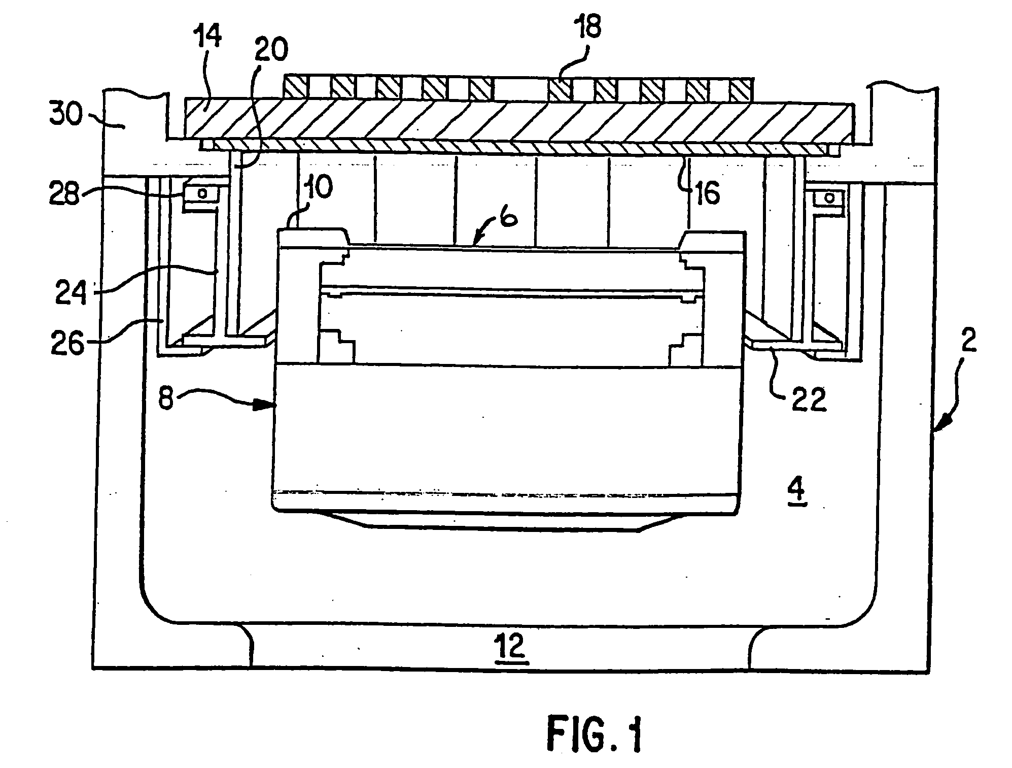
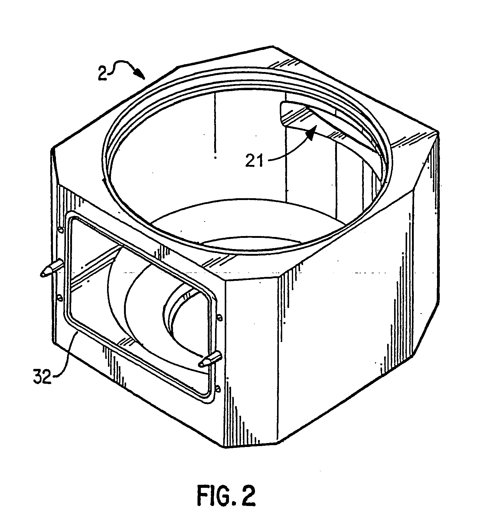
[0029] According to the invention, a plasma processing chamber having improved process drift control is provided. The improved process drift control is achieved by use of one or more parts in the chamber of a part having a surface thereof exposed to the interior space, the part having free silicon contained therein and a protective layer on the surface which protects the silicon from being attacked by the plasma in the interior. The free silicon can be silicon impregnated into a porous SiC body, the silicon filling the porosity to minimize undesirable process effects and increase electrical conductivity which is useful for lowering the RF impedance of the part.

[0030] The part can have any desired configuration such as that of a wafer passage insert, a chamber wall, a substrate support, an electrode, a showerhead, etc. According to a preferred embodiment, the part comprises a slip cast silicon carbide part which has been backfilled or impregnated with silicon and the protective coat...


PUM

PropertyMeasurementUnit
resistivityaaaaaaaaaa
thicknessaaaaaaaaaa
resistivityaaaaaaaaaa

Abstract

A plasma processing chamber including a slip cast part having a surface thereof exposed to the interior space of the chamber. The slip cast part includes free silicon contained therein and a protective layer on the surface which protects the silicon from being attacked by plasma in the interior space of the chamber. The slip cast part can be made of slip cast silicon carbide- coated with CVD silicon carbide. The slip cast part can comprise one or more parts of the chamber such as a wafer passage insert, a monolithic or tiled liner, a plasma screen, a showerhead, dielectric member, or the like. The slip cast part reduces particle contamination and reduces process drift in plasma processes such as plasma etching of dielectric materials such as silicon oxide.

Description

FIELD OF THE INVENTION [0001] The invention relates to semiconductor processing equipment and more particularly to improved process drift control during processing such as plasma etching of semiconductor substrates. BACKGROUND OF THE INVENTION [0002] In the field of semiconductor processing, vacuum processing chambers are generally used for etching and chemical vapor deposition (CVD) of materials on substrates by supplying an etching or deposition gas to the vacuum chamber and application of an RF field to the gas to energize the gas into a plasma state. Examples of parallel plate, transformer coupled plasma (TCPâ„¢) which is also called inductively coupled plasma (ICP), and electron-cyclotron resonance (ECR) reactors and components thereof are disclosed in commonly owned U.S. Pat. Nos. 4,340,462; 4,948,458; 5,200,232 and 5,820,723. Because of the corrosive nature of the plasma environment in such reactors and the requirement for minimizing particle and / or heavy metal contamination, i...

Claims


Application Information

Patent Timeline
07 Jul 2005
Publication
US20050145176A1
IPC
H01J37/32
CPC
H01J37/32495; H01L21/3065
Inventors
WICKER, THOMAS E.