Tandem thin-film photoelectric transducer and its manufacturing method

a technology of photoelectric converter and thin film, which is applied in the direction of coating, chemical vapor deposition coating, semiconductor devices, etc., can solve the problems of limited amount of photoelectric conversion, insufficient light absorption in a longer wavelength range, and the effect of increasing the conversion efficiency

Inactive Publication Date: 2005-07-07
KANEKA CORP
View PDF4 Cites 80 Cited by
  • Summary
  • Abstract
  • Description
  • Claims
  • Application Information

AI Technical Summary

Benefits of technology

[0017] In view of the above-described circumstances of the prior art, a main object of the present invention is to further improve the conversion efficiency (Eff.) of the tandem thin film photoelectric converter.
[0019] In this way, by providing the uneven surface geometry having the specified average peak-to-peak pitch on the intermediate layer having the specified thickness, it becomes possible to dramatically improve the light trapping effect of the photoelectric conversion units on both sides of the intermediate layer to achieve high photoelectric conversion efficiency. Specifically, light entering the photoelectric converter is partially reflected by the intermediate layer to the front unit to increase output current of the front unit, while in the rear unit area, light having passed through the intermediate layer is then scattered by the uneven surface geometry of the intermediate layer to be trapped between the back electrode and the intermediate layer.
[0020] In addition to the fine surface unevenness of the intermediate layer, an uneven geometry may also be provided on the surface of the transparent electrode to further improve the light trapping effect. That is, it is possible to advantageously improve the light trapping effect by the uneven surface of the transparent electrode itself, and then the light trapping effect of the intermediate layer can also be improved by superposing on the first uneven surface geometry inherent in the intermediate layer a second uneven surface geometry caused by the uneven surface geometry of the transparent electrode.

Problems solved by technology

However, these conductive layers are inactive layers which do not contribute to photoelectric conversion.
Consequently, when photoelectric conversion material is provided as a thin film, sufficient light absorption may not be achieved in a longer wavelength range where the light absorption coefficient is small and the amount of photoelectric conversion is limited by the thickness of the photoelectric conversion layer.
That is, the optical deterioration becomes more significant as the thickness of the amorphous silicon layer is increased.
However, vapor deposition and EB evaporation are not so suitable for forming a film of a large area and they make it difficult to form an intermediate layer having uniform thickness and quality over a photoelectric conversion unit of a large area.
As such, large kinetic energy of atoms and radicals reaching the underlayer surface is liable to damage the underlayer during formation of the intermediate layer, and thus it cannot be guaranteed that the intermediate layer improves the properties of the photoelectric converter.
In the hybrid thin film photoelectric converter, the short-circuited current density is typically limited by the amount of absorbed light in the amorphous silicon photoelectric conversion unit.
However, an excessively large thickness of the photoelectric conversion layer is not preferable, because it increases influence of film quality of the layer on the conversion efficiency to a non-negligible level.
Also, the photoelectric conversion layer with an excessively large thickness is not preferable, since it requires a longer time for deposition and reduces productivity of the photoelectric converter.
A further problem is that the underlying photoelectric conversion unit may be damaged during formation of the intermediate layer and then the interface joining this unit and the intermediate layer may be degraded, causing reduction in fill factor (F.F.) of the entire photoelectric converter.

Method used


Image

  • Tandem thin-film photoelectric transducer and its manufacturing method
  • Tandem thin-film photoelectric transducer and its manufacturing method
  • Tandem thin-film photoelectric transducer and its manufacturing method

Examples


example 1

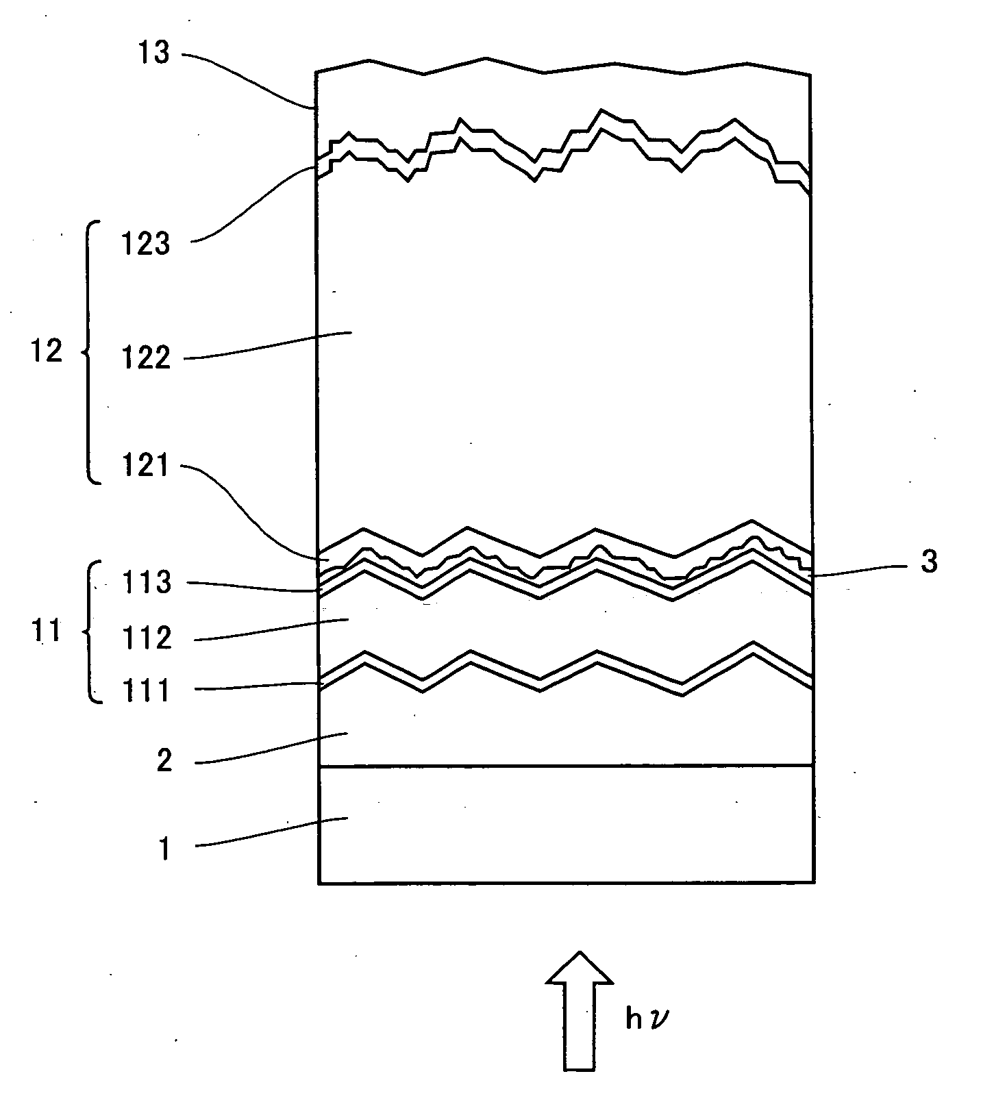
[0053] A hybrid thin film photoelectric converter as shown in FIG. 1 was fabricated as Example 1. On a square glass substrate 1 having a thickness of 1.1 mm and a side length of 127 mm, a tin oxide film having an average thickness of 800 nm and having a pyramidal surface unevenness was deposited by thermal CVD to form a transparent electrode 2. Obtained transparent electrode 2 had a sheet resistance of about 9 Ω / □. When glass substrate 1 with transparent electrode 2 formed thereon was illuminated by a standard light C having a specified wavelength distribution, its measured haze factor was 12%. Then, the average height difference d of unevenness on the upper surface of transparent electrode 2 was about 100 nm. An amorphous silicon photoelectric conversion unit 11 was formed on transparent electrode 2 by plasma CVD. Unit 11 was composed of a p-type amorphous silicon-carbide layer 111 of 15 nm thickness, an i-type amorphous silicon photoelectric conversion layer 112 of 0.25 μm thickne...

example 2

[0061] In Example 2, a hybrid thin film photoelectric converter was fabricated in a manner similar to that in Example 1, except that a zinc oxide film of 30 nm thickness was deposited at a substrate temperature of 150° C. by sputtering to form intermediate layer 3.

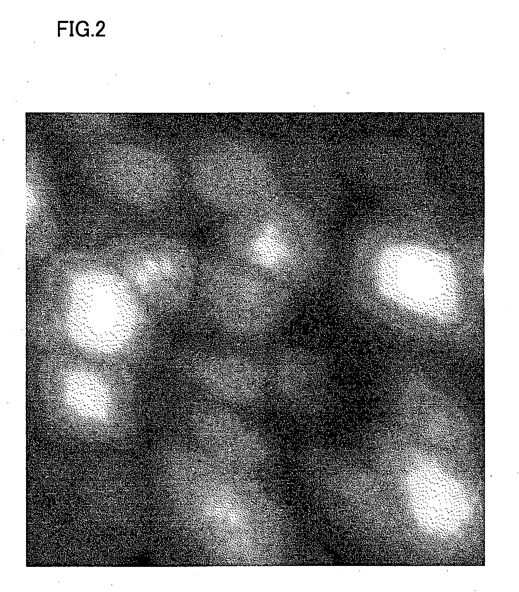
[0062]FIG. 5 shows an AFM image of the upper surface (in a rectangular area of 1.5 μm×9.0 μm) of a zinc oxide film formed on a flat glass plate under sputtering conditions similar to those for intermediate layer 3 of Example 2, and FIG. 6 shows an uneven surface geometry measured by AFM along a broken line in FIG. 5. In the graph of FIG. 6, each scale of the lateral axis indicates 0.1 μm and each scale of the vertical axis indicates 5 nm. In the uneven surface geometry in FIG. 6, the distance between E and F that corresponds to a diameter of one typical small projection (corresponding to a pitch measured parallel to the glass plate between two adjacent depressions) is 35.2 nm. When a square area of the zinc oxide film wit...

example 3

[0064] In Example 3, a hybrid thin film photoelectric converter was fabricated in a manner similar to that in Example 1, except that i-type crystalline silicon photoelectric conversion layer 122 had a thickness of 2.7 μm.

[0065] When output characteristics of a silicon-based thin film photoelectric converter (with a light reception area of 1 cm2) obtained in Example 3 were measured at 25° C. by illuminating with light of AM1.5 at a light intensity of 100 mW / cm2, the converter had a Voc of 1.36V, a Jsc of 12.2 mA / cm2, an F.F. of 73.6%, and a conversion efficiency of 12.2%.


PUM

PropertyMeasurementUnit
thicknessaaaaaaaaaa
thicknessaaaaaaaaaa
thicknessaaaaaaaaaa

Abstract

A tandem thin film photoelectric converter includes a transparent electrode, a plurality of photoelectric conversion units and back electrode deposited in sequence on a transparent insulating substrate. An intermediate layer for partially reflecting and transmitting light is inserted along at least one interface between the plurality of photoelectric conversion units. The intermediate layer has an average thickness in the range of 10 to 90 nanometers. The upper surface of the intermediate layer includes an uneven surface geometry having an average peak-to-peak pitch in the range of 10 to 50 nanometers.

Description

TECHNICAL FIELD [0001] The present invention relates to improvement in photoelectric conversion efficiency of a thin film photoelectric converter, and more particularly to improvement in conversion efficiency of a tandem thin film photoelectric converter including a plurality of stacked photoelectric conversion units. In the present specification, terms “crystalline” and “microcrystalline” are used also for a state partially including amorphous regions, as generally used in the field of the art. BACKGROUND ART [0002] In order to reduce costs of photoelectric converters and at the same time to improve conversion efficiencies thereof, thin film photoelectric converters which are also preferable in view of saving natural resources have attracted attention in recent years and have been developed with intensive effort. Thin film photoelectric converters are expected to be employed in various applications such as solar batteries, optical sensors, displays and the like. An amorphous silico...

Claims


Application Information

Patent Timeline
Patent Type & Authority Applications(United States)
IPC IPC(8): C23C16/40H01L31/0236H01L31/04H01L31/06H01L31/075H01L31/076H01L31/077
CPCH01L31/0236Y02E10/548H01L31/076H01L31/02363H01L31/02366Y02E10/547
Inventor FUKUDA, SUSUMUTAWADA, YUKOKOI, YOUHEIYAMAMOTO, KENJI
Owner KANEKA CORP
Why Eureka
Try Eureka