

Photoresist composition
a technology of composition and resist, applied in the direction of photosensitive material auxillary/base layer, nuclear engineering, electrical equipment, etc., can solve the problems of high etch rate, inability to use open-chain aliphatic resins, and resist materials applicable for 248 nm to achieve the effect of reducing the etch ra
- Summary
- Abstract
- Description
- Claims
- Application Information
AI Technical Summary
Benefits of technology
Problems solved by technology
Method used
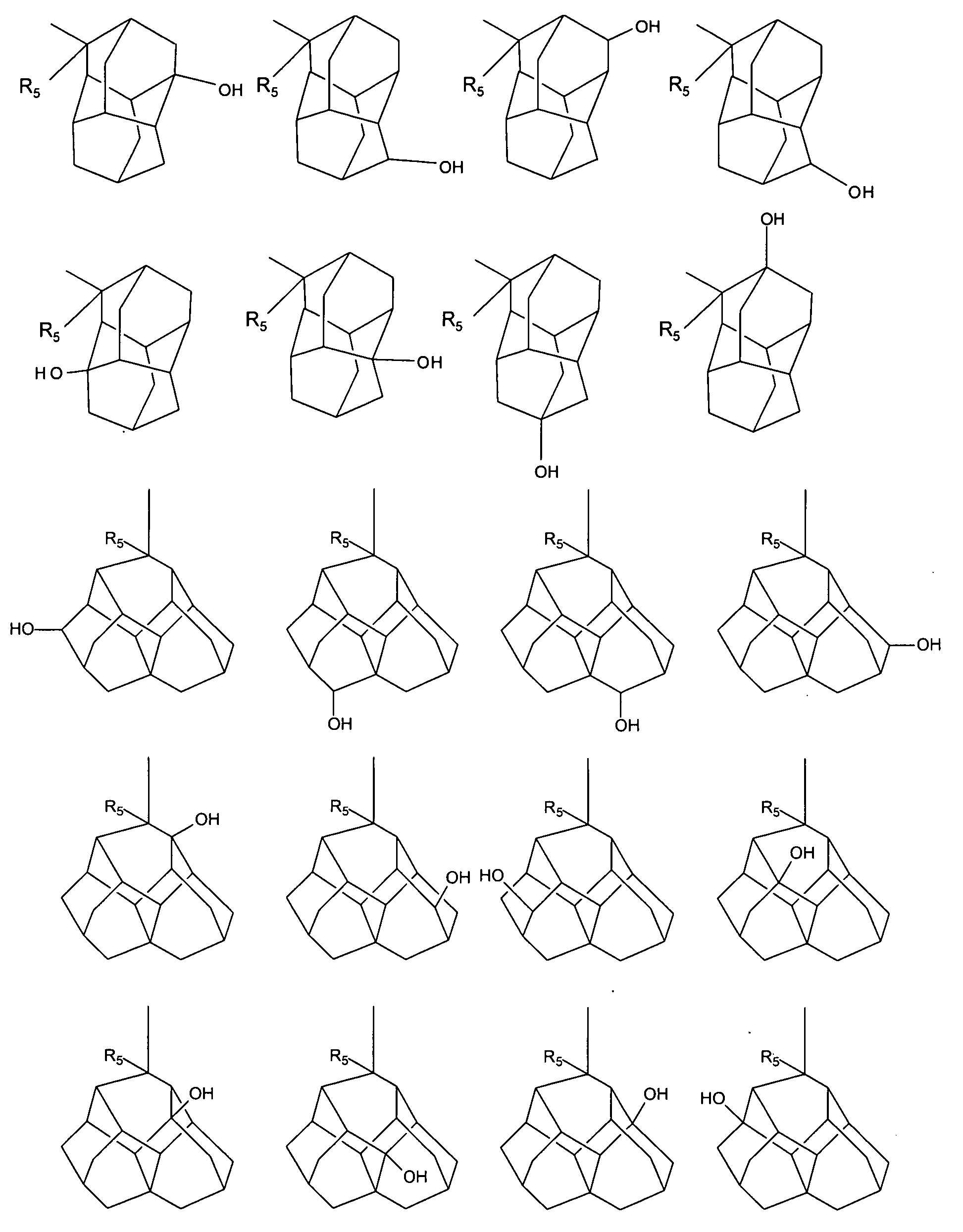
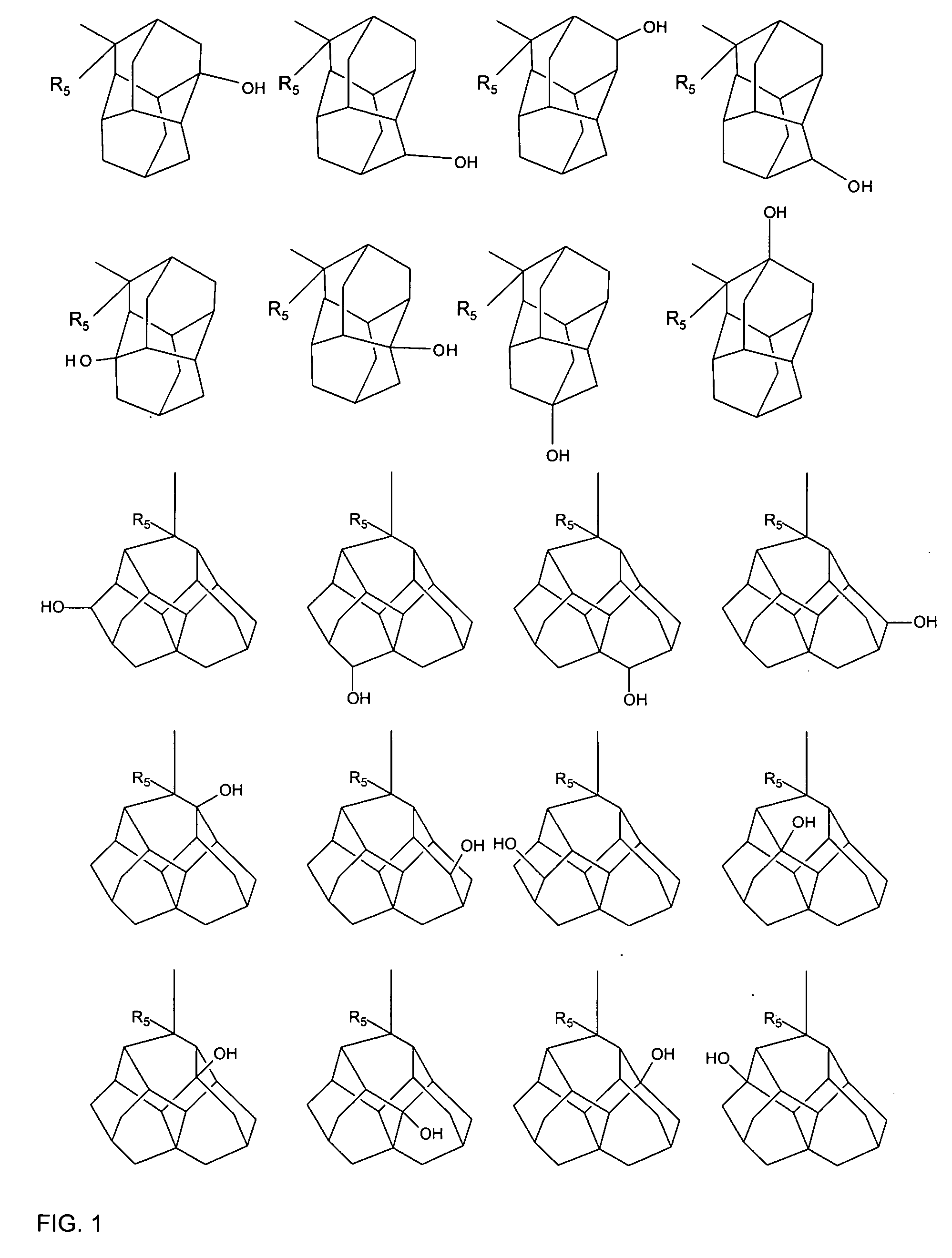
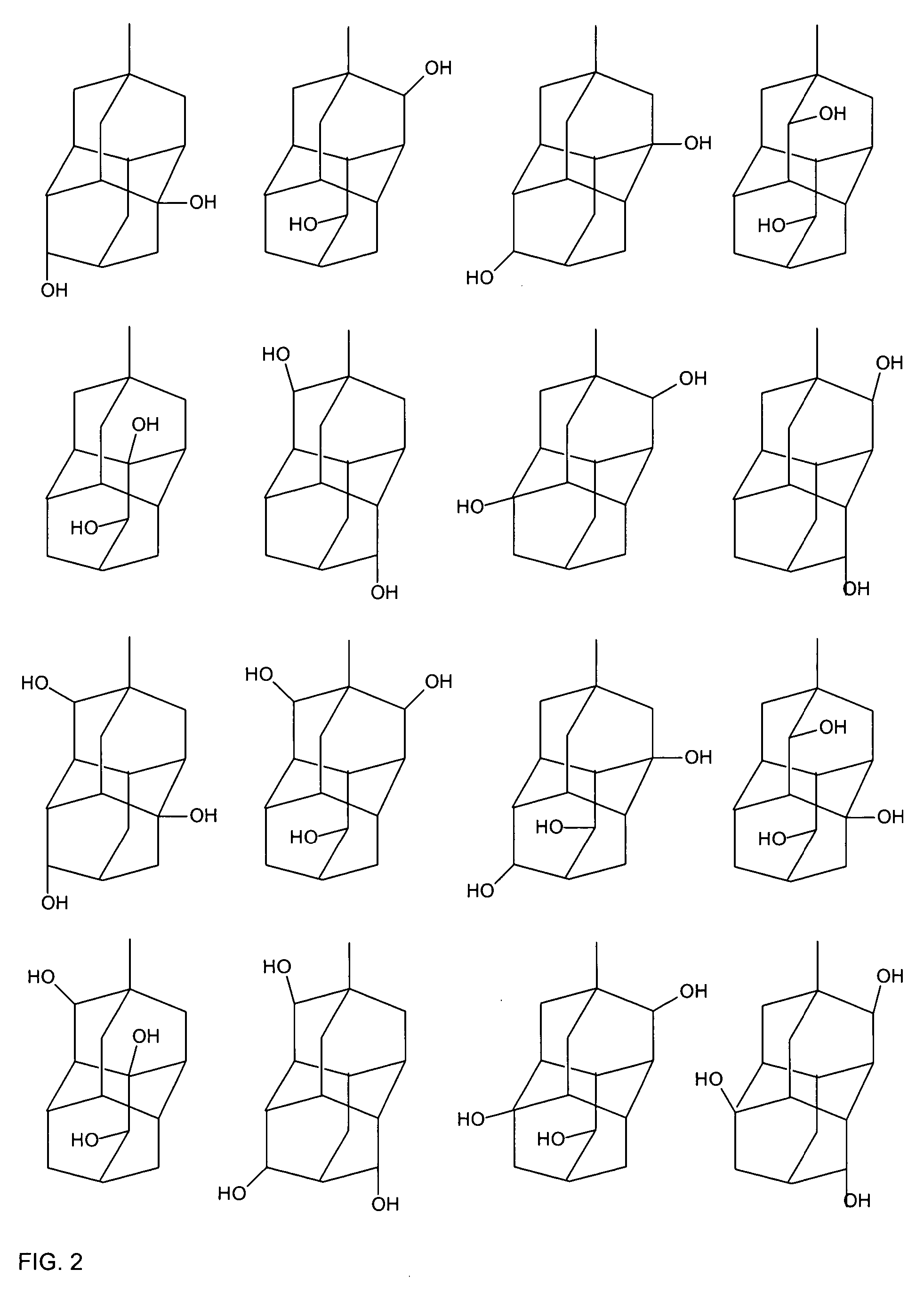
Image

Examples
example 1
[0072] General polymerization procedure for polymers not containing maleic anhydride:
[0073] A copolymer is synthesized from the target monomer mixture in the presence of 15 weight % of AlBN in tetrahydrofuran (THF) at 30% solids. The reaction mixture is thoroughly deoxygenated by passing a stream of n itrogen through the reaction mixture prior to heating, then maintaining a nitrogen atmosphere over the polymerization during the remaining reaction. The reaction mixture is held at a slow reflux for 8 hours, then it is allowed to cool down and is diluted with a third of its volume of methanol. It is then added dropwise and with vigorous stirring to a large excess of methanol, yielding a fine white precipitate which is then isolated by suction filtration. The filtercake is re-dissolved in THF and precipitated into a large excess of hexane, heptane, or petrol ether. The filtration and re-precipitation steps into methanol and alkane are repeated a second time. The polymer is then dried o...
example 2
[0074] General polymerization procedure for polymers containing maleic anhydride:
[0075] A copolymer is synthesized from the target monomer mixture in the presence of 2 weight % of AlBN in tetrahydrofuran (THF) at 30% solids. The reaction mixture is thoroughly deoxygenated by passing a stream of dry nitrogen through the reaction mixture prior to heating. Following deoxygenation, the reaction is carried out under pressure for 18 hours, where the starting pressure is about 48,260 Pascals (7 psi). Following depressurization, the polymer is isolated from diethyl ether (1 / 10 v / v ratio) by two successive precipitations. The polymer is then dried overnight in a vacuum oven at 40° C. For the monomers in question, typical isolated polymer yields in this procedure are from between 55 to 65%.
example 3
[0076] General photoresist formulation procedure:
[0077] The polymer of Example 1 or 2 is dissolved in propylene glycol monomethyl ether acetate (PGMEA) as an 8% solution (w / w). Triphenylsulfonium nonafluorobutane-sulfonate (TPS-Nf) is added at a level of 2% of the polymer weight, followed by an amount of diethanolamine (in the form of a 1% PGMEA solution) equivalent to 30 mole-% of the TPS-Nf. A small amount (about 0.001%) of FC-4430 surfactant (fluoroaliphatic polymeric ester, supplied by 3M Corporation, St. Paul, Minn.) is added in order to suppress striations and improve coating uniformity. The formulation is mixed overnight by agitation and is then filtered through depth and membrane filters, with the last filter having a pore size rating of 0.05 μm. If necessary additional solvent is added to allow the formulation to be coated at a film thickness of 280 nm.
PUM
| Property | Measurement | Unit |
|---|---|---|
| of wavelength in the range | aaaaa | aaaaa |
| wavelength | aaaaa | aaaaa |
| wavelength | aaaaa | aaaaa |
Abstract
Description
Claims
Application Information