
Electrophotographic photoconductor, and image formation method, image formation apparatus, and process cartridge for image formation apparatus using the same

Active Publication Date: 2005-07-21
RICOH KK
View PDF34 Cites 76 Cited by
  • Summary
  • Abstract
  • Description
  • Claims
  • Application Information

AI Technical Summary

Benefits of technology

[0022] One of the objects of the present invention to provide an electrophotographic photoconductor that can realize excellent service durability and stable electrical characteristics for a long period, using a photoconductive layer with high abrasive resistance, good film surface properties, and good electrical characteristics.
[0024] Another object of the present invention is to provide an electrophotographic photoconductor that can realize excellent service durability, highly stable electrical characteristics, and high quality image formation for a long period, using a surface layer with high abrasive resistance, a smooth film surface, and littlie variation in electrical characteristics dependent on the environment.
[0026] Further objects of the present invention are to provide an image formation method, an image formation apparatus and a process cartridge for image formation apparatus using the aforementioned high quality photoconductor with a long operating life.

Problems solved by technology

From this viewpoint, since a surface layer of the organic photoconductor is based on a low-molecular-weight charge transportation material and an inactive polymer, the organic photoconductor is generally soft, and, therefore, has a disadvantage of easily causing abrasion by mechanical load from a development system or a cleaning system, when the organic photoconductor is used repeatedly in an electrophotographic process.
Such abrasion of the photoconductor lowers the sensitivity and degrades electric characteristics such as the charging property, so as to cause the lowering in image density and improper imaging such as background contamination.
Also, the damage caused by local abrasion results in insufficient cleaning, and therefore, an image with linear contamination.
Among these techniques, (1) the use of a curable binder tends to elevate a residual potential and cause lowering in image density due to a low compatibility with a charge transportation material and impurities such as a polymerization initiator and an unreacted residue.
Also, (2) the use of a polymeric charge transportation material and (3) dispersing an inorganic filler can improve abrasive resistance to some extent, but have not satisfied sufficiently the resistance required for an organic photoconductor.
Additionally, (3) dispersing an inorganic filler tends to elevate a residual potential and cause lowering in image density due to a trap existing on the surface of the inorganic filler.
Moreover, these techniques denoted by (1), (2), and (3) have not satisfied sufficiently the overall durability that includes electric durability and mechanical durability required for an organic photoconductor.
Further, when a low-molecular-weight charge transportation material is simply contained in a surface layer, there is a problem of the compatibility with the cured material, whereby the precipitation of the low-molecular-weight charge transportation material and the production of a crack can be caused to lower the mechanical strength.
Although the patent also discloses that a polycarbonate resin is contained for improving the compatibility, the content of the acryl monomers to be cured is reduced and, consequently, sufficient abrasive resistance cannot be achieved.
However, since the film thickness is small, the operating life of the photoconductor is short.
Further, the environmental stability of charging electric potential and the electric potential of a light-exposed portion is low and the values of them varies widely dependent on the environment factors such as temperature and humidity and cannot be kept at a sufficient values at present.
The photoconductor attracts attention since the photoconductor has both abrasive resistance and good electrical characteristics, but when a binder resin having no reactivity is used, the compatibility of the binder resin with a cured material produced by the reaction of the aforementioned monomers and the charge transportation material is low and layer separation or the production of surface irregularity are made at the time of cross-linking.
As the result, it is observed that the photoconductor tends to cause improper cleaning.
As described above, the binder resin disturbs the curing of the monomers.
Further, the patent discloses a two-functional monomer as the monomer used in the photoconductor but sufficient cross-link density cannot be obtained by the two-functional monomers since the number of functional groups of the monomer is small and the photoconductor does not satisfy the sufficient abrasive resistance.
Also, when the binder resin having reactivity, due to the small number of functional groups contained in the monomer and the binder resin, it is difficult to balance the extent of monomer coupling in the charge transportation material and the cross-link density of the charge transportation material, and the electrical characteristics and the abrasive resistance are insufficient.
However, since the bulky hole transportation compound in the photoconductive layer has more than one chain-polymerizable functional group, distortion is caused and the internal stress increases in the cured compound.
As the result, the surface layer may easily become rough or produce a crack with time, so that the surface layer does not have sufficient durability.
Thus, the photoconductor having a cross-linked photoconductive layer obtained by chemically bonding the electron transporting structures in these conventional techniques does not have the sufficient overall characteristics at present.

Method used


Image

  • Electrophotographic photoconductor, and image formation method, image formation apparatus, and process cartridge for image formation apparatus using the same
  • Electrophotographic photoconductor, and image formation method, image formation apparatus, and process cartridge for image formation apparatus using the same
  • Electrophotographic photoconductor, and image formation method, image formation apparatus, and process cartridge for image formation apparatus using the same

Examples


example 1-1

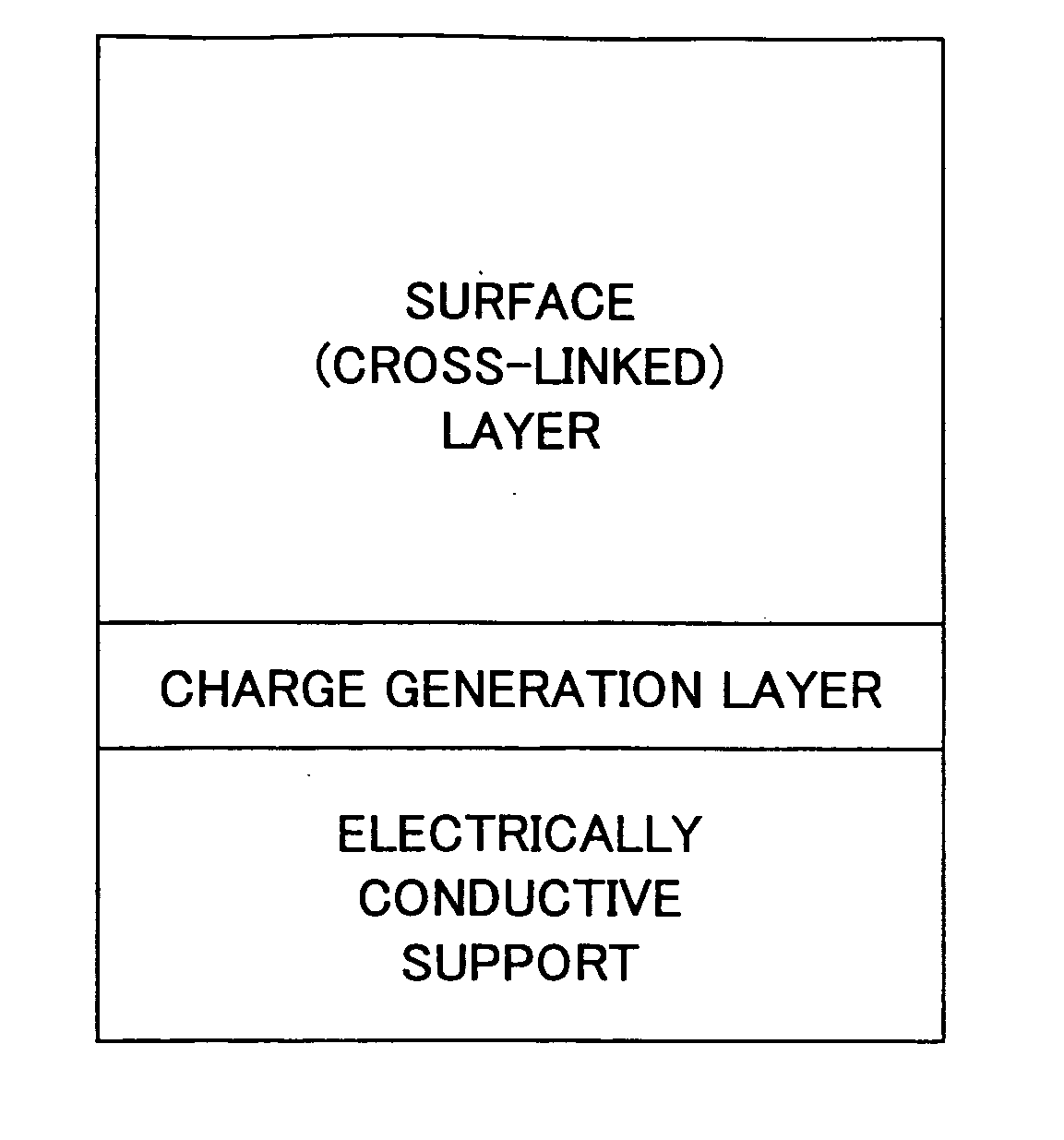
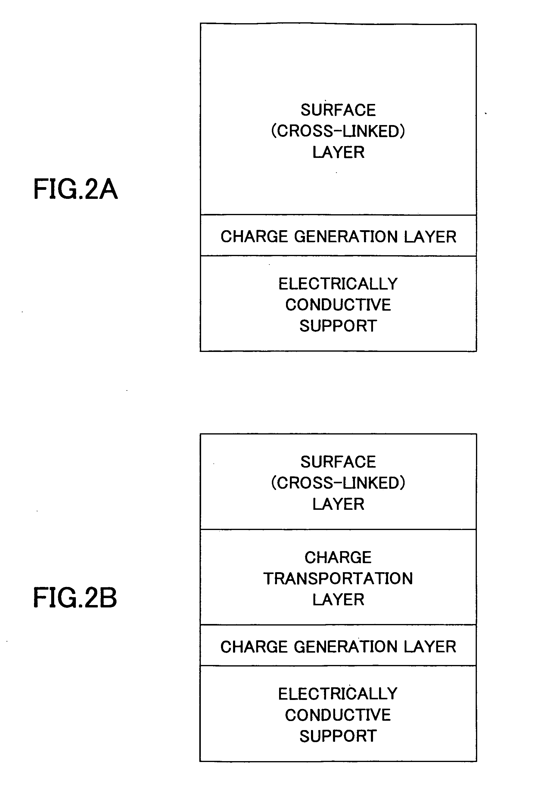
[0250] Coating liquid for underlying layer, coating liquid for charge generation layer, and coating liquid for charge transportation layer, which had the following compositions, were applied on an aluminum cylinder in the order by dip coating and dried so as to form 3.5 μm of an underlying layer, 0.2 μm of an charge generation layer, and 23 μm of an charge transportation layer.

[0251] {Coating Liquid for Underlying Layer}

[0252] Alkyd resin: 6 parts

[0253] (Beckosol 1307-60-EL produced by DAINIPPON INK AND CHEMICALS, INCORPORATED)

[0254] Melamine resin: 4 parts

[0255] (Superbeckamine G-821-60 produced by DAINIPPON INK AND CHEMICALS, INCORPORATED)

[0256] Titanium oxide: 40 parts

[0257] (CR-EL: ISHIHARA SANGYO KAISHA, LTD.)

[0258] Ethyl methyl ketone: 50 parts

[0259] {Coating Liquid for Charge Generation Layer}

[0260] Bisazo pigment having the following structure: 2.5 parts

[0261] Polyvinyl butyral: 0.5 parts

[0262] (XYHL produced by UCC)

[0263] Cyclohexanone: 200 parts

[0264] Ethyl me...

example 1-2

[0284] An electrophotographic photoconductor was produced similar to example 1-1 except that the free-radical-polymerizable monomer having no electron transporting structure contained in the coating liquid for cross-linked surface layer in example 1-1 was changed to the following compound.

[0285] Caprolactone-modifieddi-penta-erythritol hexaacrylate

[0286] (KAYARAD DPCA-60 produced by NIPPON KAYAKU CO., LTD.)

example 1-3

[0287] An electrophotographic photoconductor was produced similar to example 1-1 except that the free-radical-polymerizable monomer having no electron transporting structure contained in the coating liquid for cross-linked surface layer in example 1-1 was changed to the following compound.

[0288] EO-modified di-penta-erythritol hexaacrylate

[0289] (KAYARAD DPEA-12 produced by NIPPON KAYAKU CO., LTD.)

[0290] (Herein, the mean average of n is 12.)


PUM

PropertyMeasurementUnit
Fractionaaaaaaaaaa
Fractionaaaaaaaaaa
Fractionaaaaaaaaaa

Abstract

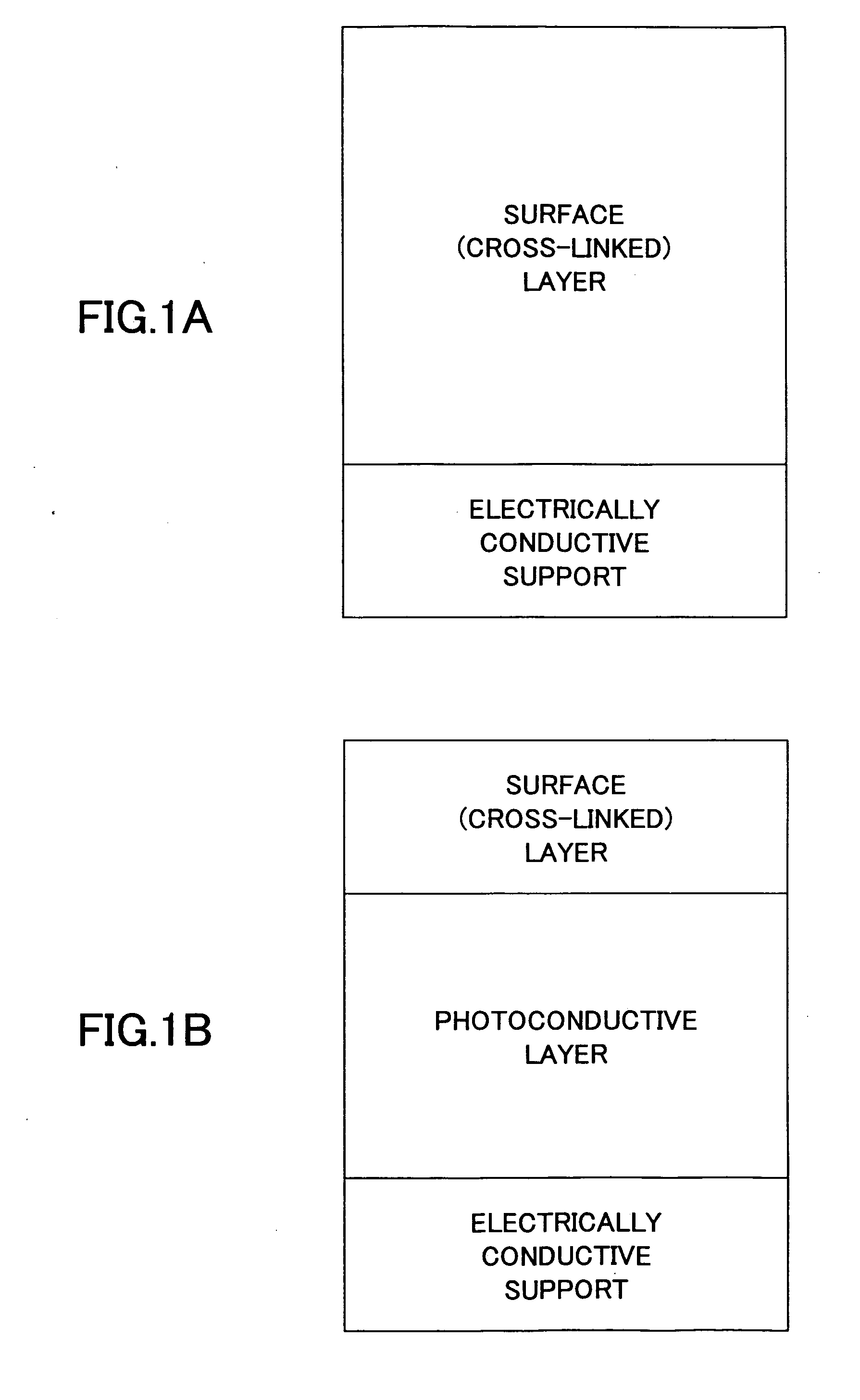
An electrophotographic photoconductor having at least a photoconductive layer on an electrically conductive support, in which a surface layer of the photoconductive layer can be obtained by curing at least a free-radical-polymerizable monomer having no electron transporting structure, represented by general formula (A) and a one-functional free-radical-polymerizable compound having an electron transporting structure, wherein R71, R72, R73, R74, R75, and R76 are described in the specification.

Description

BACKGROUND OF THE INVENTION [0001] 1. Field of the Invention [0002] First, the present invention relates to an electrophotographic photoconductor that can realize excellent service durability, stable electrical characteristics, and high quality image formation for a long period, using a photoconductive layer with high abrasive resistance, good film surface properties, and good electrical characteristics. [0003] Second, the present invention relates to an electrophotographic photoconductor that can realize excellent service durability, stable electrical characteristics, and high quality image formation for a long period, using a surface layer with high abrasive resistance, a smooth film surface, and littlie variation in electrical characteristics dependent on the environment. [0004] Further, the present invention relates to an image formation method, an image formation apparatus and a process cartridge for image formation apparatus using the aforementioned high quality photoconductor...

Claims


Application Information

Patent Timeline
IPC IPC(8): G03G5/05G03G5/07G03G5/147
CPCG03G5/0532G03G5/0542G03G5/0546G03G5/0592G03G5/071G03G5/14791G03G5/14717G03G5/1473G03G5/14734G03G5/14739G03G5/076G03G5/072G03G5/0745G03G5/0732G03G5/074
Inventor YANAGAWA, YOSHIKIIKUNO, HIROSHILI, HONGGUONAGAI, KAZUKIYOTAMURA, HIROSHISUZUKI, TETSUROTODA, NAOHIROKAWASAKI, YOSHIAKI
Owner RICOH KK
Learn More