Hybrid active matrix thin-film transistor display

Inactive Publication Date: 2005-08-04
ITUS
View PDF10 Cites 18 Cited by
  • Summary
  • Abstract
  • Description
  • Claims
  • Application Information

AI Technical Summary

Problems solved by technology

Although significant technological progress has been made in recent years, LCDs still have some drawbacks and limitations that pose considerable restraints.
First, LCD technology is rather complex, which results in a high manufacturing cost and price of the product.
Other deficiencies, such as small viewing angle, low brightness and relatively narrow temperature range of operation, make application of the LCDs difficult in many high market value areas such as car navigation devices, car computers, and mini-displays for cellular phones.
One limitation associated with plasma displays is that the pixel cells for plasma discharge cannot be made very small without affecting neighboring pixel cells.
This is why the resolution in plasma FPD is poor for small format displays and becomes more efficient as the display size increases above 30″ diagonally.
Another limitation associated with plasma displays is that they tend to be thick as compared to FPDs.
Further, they tend to be heavy and generate high temperatures.
However, after ten years of effort FEDs are not yet in the market.
FED mass production has been delayed for several reasons.
The technology for fabricating the metal tips, together with necessary controlling gates, is rather complex.
Another difficulty associated with FED mass production relates to the lifetime of FEDs.
Electrons striking the phosphors result in phosphor molecule dissociation and formation of gases, such as sulfur oxide and oxygen, in the vacuum chamber.
The gas molecules reaching the tips cloud or shield the electric field resulting in a reduction of the efficiency of electron emission from the tips.
A second group of gases, produced by electron bombardment, contaminates the phosphor surface and forms undesirable energy band bending at the phosphor surface.
This, however, creates another problem.
99, which further complicates display fabrication.
The metal tip-like emitters and holes in the controlling gate, which are less than 1 μm in diameter, are expensive and time consuming to manufacture, hence they are not readily suited for mass production.
The anode electrode is fabricated on the same substrate, and is oriented normally to the substrate plane, making it unsuitable for display functions.
The anode electrode, however, requires a second plate which significantly complicates the fabrication of the display.
Another limitation of FEDs is that the emitter films, including the diamond film and the insulator film, are grown on a phosphor film.
The phosphor film is known to have a very rough surface morphology that makes it unsuitable for any further film deposition.

Method used


Image

  • Hybrid active matrix thin-film transistor display
  • Hybrid active matrix thin-film transistor display
  • Hybrid active matrix thin-film transistor display

Examples


second embodiment

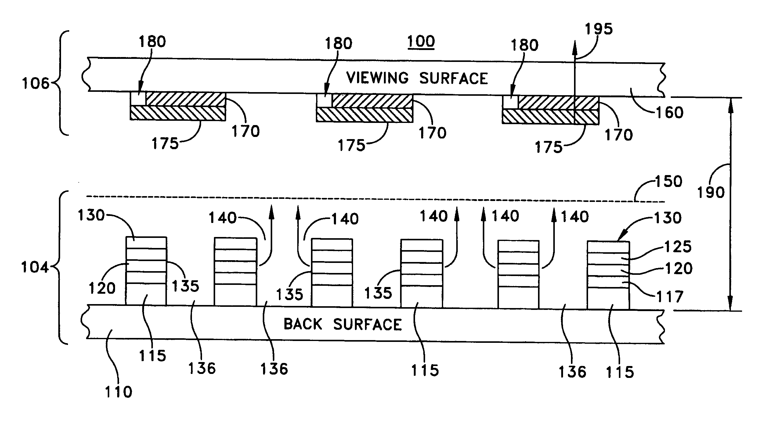
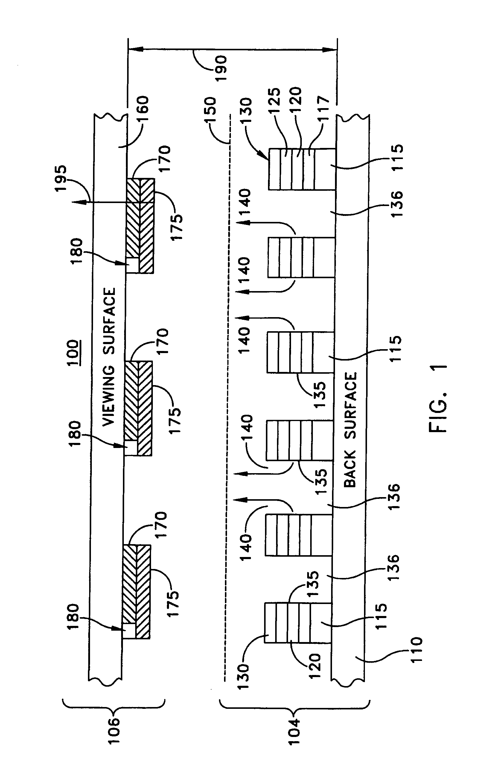
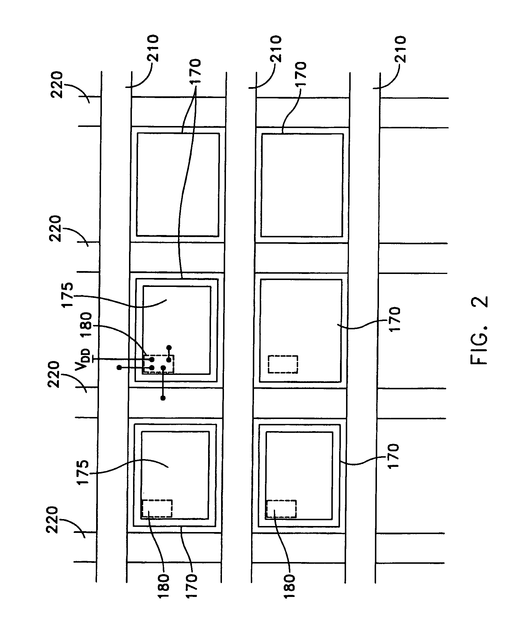
[0061]FIG. 4 illustrates the display. In this embodiment, the TFT anode structure shown in FIG. 2 is deposited on substrate 110. In this case, a material such as poly-silicon or amorphone silicon, may be deposited on substrate 110, that allows for the fabrication of row lines 210 (not shown), column lines 220 (not shown), conductive pad 170 and TFT circuit 180 onto substrate 110 in row / column matrix as shown in FIG. 2. Phosphor layer 175 may then be deposited on corresponding conductive pads 170.

[0062] In one aspect a silicon (Si) single crystal wafer may be used for the active matrix circuitry, wherein the Si wafer is attached to a glass substrate. In this case, the phosphor pads are also made on the Si wafer.

[0063] Cathode 104 is fabricated on viewing surface 160 and emitter layer 120 and conductive layer 130 operate to draw electrons from edges 135 of emitter layer 120. Emitter layer 120 and conductive layer 130 occupy a significantly small portion of the viewing glass area to a...

first embodiment

[0076] Alternatively, referring now also to FIGS. 13A-14, TFT circuits 180 may include an amplification stage (FIGS. 13A-13C) and a pixel circuit stage (FIG. 14). a schematic circuit representation of a TFT amplification stage 1300A suitable for use in display 1100 of FIG. 11 is shown in FIG. 13A. Stage 1300A may be characterized as a two n-channel transistor configuration. Stage 1300A includes a first n-channel transistor M1 having gate and drain terminals coupled to a known voltage such as Vdd or about +40V. A source terminal of transistor M1 is coupled to a drain terminal of a second n-channel transistor M2 and an input for the pixel circuit stage. A gate terminal of transistor M2 may have a column driver data signal, such as a 0-5V signal, provided thereon. A source terminal of transistor M2 may have another known voltage VTH, such as about 3 to about 5 volts, provided thereon.

[0077] According to a second embodiment, a schematic circuit representation of a TFT amplification sta...

third embodiment

[0078] a schematic circuit representation of a TFT amplification stage 1300C suitable for use in the display 1100 of FIG. 11 is shown in FIG. 13C. Stage 1300C may be characterized as a one p-channel, two n-channel transistor configuration. In operation, stage 1300C may serve to increase a realized output swing and power efficiency. Stage 1300C includes a p-channel transistor M1 having a source terminal coupled to a known voltage such as Vdd or about +40V. A gate terminal of transistor M1 may be provided with another known voltage V1, such as a voltage of about 36 or 37 volts, or a voltage less than about 40 volts. A drain terminal of transistor M1 is coupled to a drain terminal of a first n-channel transistor M2 and an input for the pixel circuit stage. A gate terminal of transistor M2 may have a column driver data signal, such as a 0-5V signal, provided thereon. A source terminal of transistor M2 may have another known voltage VTH provided thereon. A second n-channel transistor M5...


PUM


Abstract

A field emission display comprises an anode comprising a matrix of pixels and a cathode comprising an insulating layer defining a plurality of wells having a conductor therein. A first conductive layer forms a plurality of conductive pads, each of the conductive pads corresponding to one of the wells. A plurality of nanostructures are electrically coupled to the conductive pads. A second conductive layer is formed over the insulating layer and provides a plurality of gate electrodes. When a potential between the conductive pads and gate electrodes exceeds a threshold voltage, the nanostructures emit electrons that impinge on the pixels.

Description

RELATED APPLICATIONS [0001] This application is a continuation-in-part of: U.S. patent application Ser. No. 10 / 763,030, entitled “Hybrid Active Matrix Thin-Film Transistor Display,” filed on Jan. 22, 2004, U.S. patent application Ser. No. 10 / 782,580, entitled “Hybrid Active Matrix Thin-Film Transistor Display,” filed on Feb. 19, 2004, and U.S. patent application Ser. No. 10 / 102,472, entitled “Pixel Structure for an Edge-Emitter Field-Emission Display,” filed Mar. 20, 2002, the entire disclosures of each of which are all hereby incorporated by reference herein.FIELD OF THE INVENTION [0002] This application is related to the field of vacuum displays and more specifically to flat panel displays using Thin Film Transistor (TFT) technology. BACKGROUND OF THE INVENTION [0003] Flat panel display (FPD) technology is one of the fastest growing technologies in the world with a potential to surpass and replace Cathode Ray Tubes (CRTs) in the foreseeable future. As a result of this growth, a la...

Claims


Application Information

Patent Timeline
IPC IPC(8): H01J1/02
CPCH01J1/304H01J2329/0455H01J2201/30469H01J31/127
Inventor DISANTO, FRANK J.KRUSOS, DENIS A.SHOKHOR, SERGEY L.KASTALSKY, ALEXANDERCAMPISI, ANTHONY J.
Owner ITUS
Why Eureka
Try Eureka