Substrate attaching method

a technology of substrate and adhesive layer, which is applied in the direction of adhesive types, transportation and packaging, chemical instruments and processes, etc., can solve the problems of insufficient protection tape to support thinned semiconductor wafers, difficult stripping after bonding, and easy cracking or chipping of semiconductor wafers when the tape is pressed, etc., to achieve easy control of the thickness of the adhesive layer, easy stripping after bonding, and high softening point

Inactive Publication Date: 2005-08-04
NXP BV +1
View PDF3 Cites 67 Cited by
  • Summary
  • Abstract
  • Description
  • Claims
  • Application Information

AI Technical Summary

Benefits of technology

[0015] By conducting preliminary drying, it is possible to easily control the thickness of the adhesive layer. In order to obtain a necessary thickness, the applying step and the preliminary drying step may be repeated a plurality of times.
[0016] As the adhesive, it is preferable to employ a non-soluble macromolecular compound because water is used at the time of grinding. It is also preferable that the softening point is high because there is a high-temperature treatment step such as attachment of a DAF (Die Attach Film). Accordingly, preferable examples include a solution which is obtained by dissolving a novolac resin, an epoxy resin, an amide resin, a silicone resin, an acry

Problems solved by technology

In the case of using the protecting tape as disclosed in Document 1, cracking or chipping of the semiconductor wafer easily occur when the tape is stripped.
Also, the protecting tape is not sufficient to support the thinned semiconductor wafer.
Consequently, transfer needs to be conducted by man

Method used


Image

  • Substrate attaching method
  • Substrate attaching method
  • Substrate attaching method

Examples


Embodiment Construction

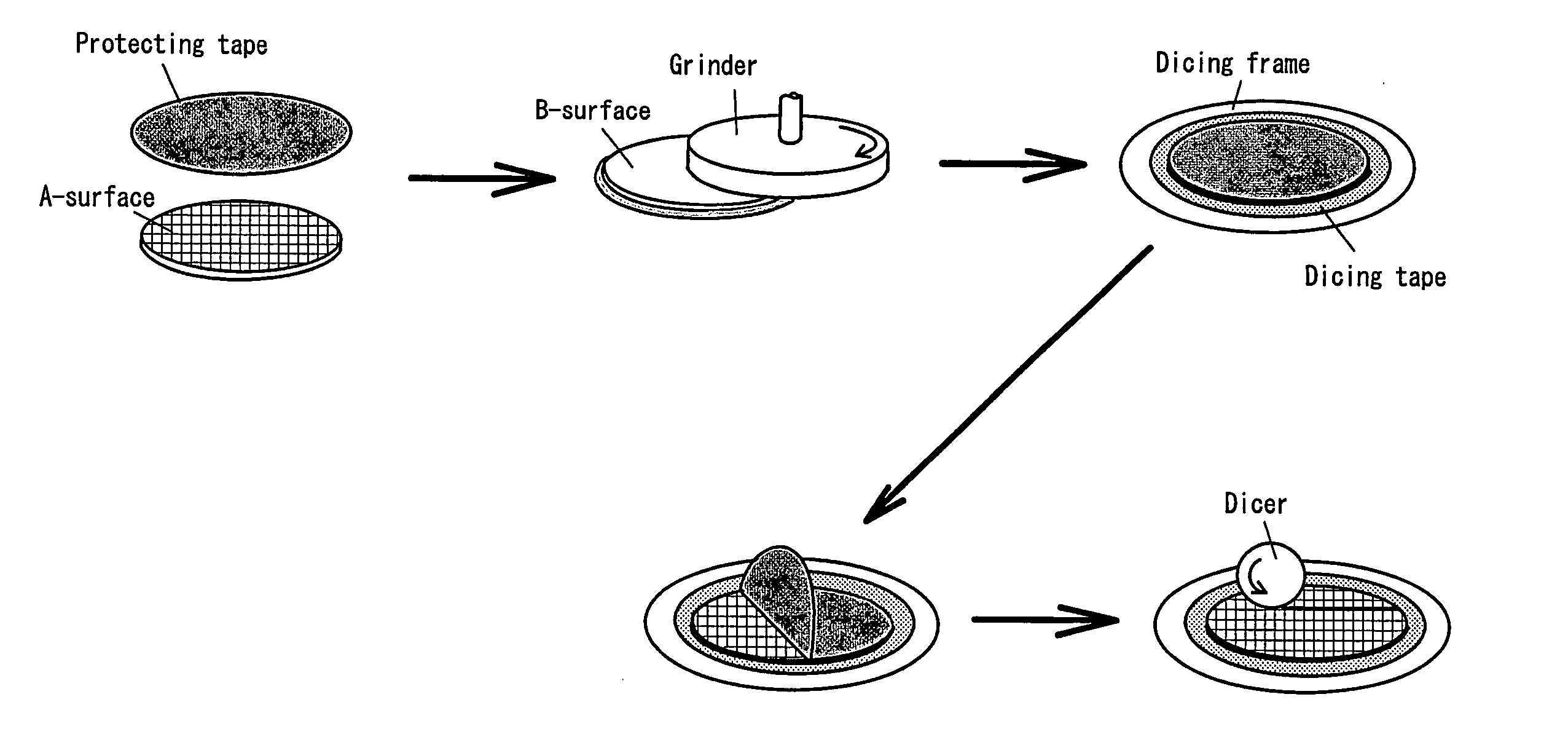
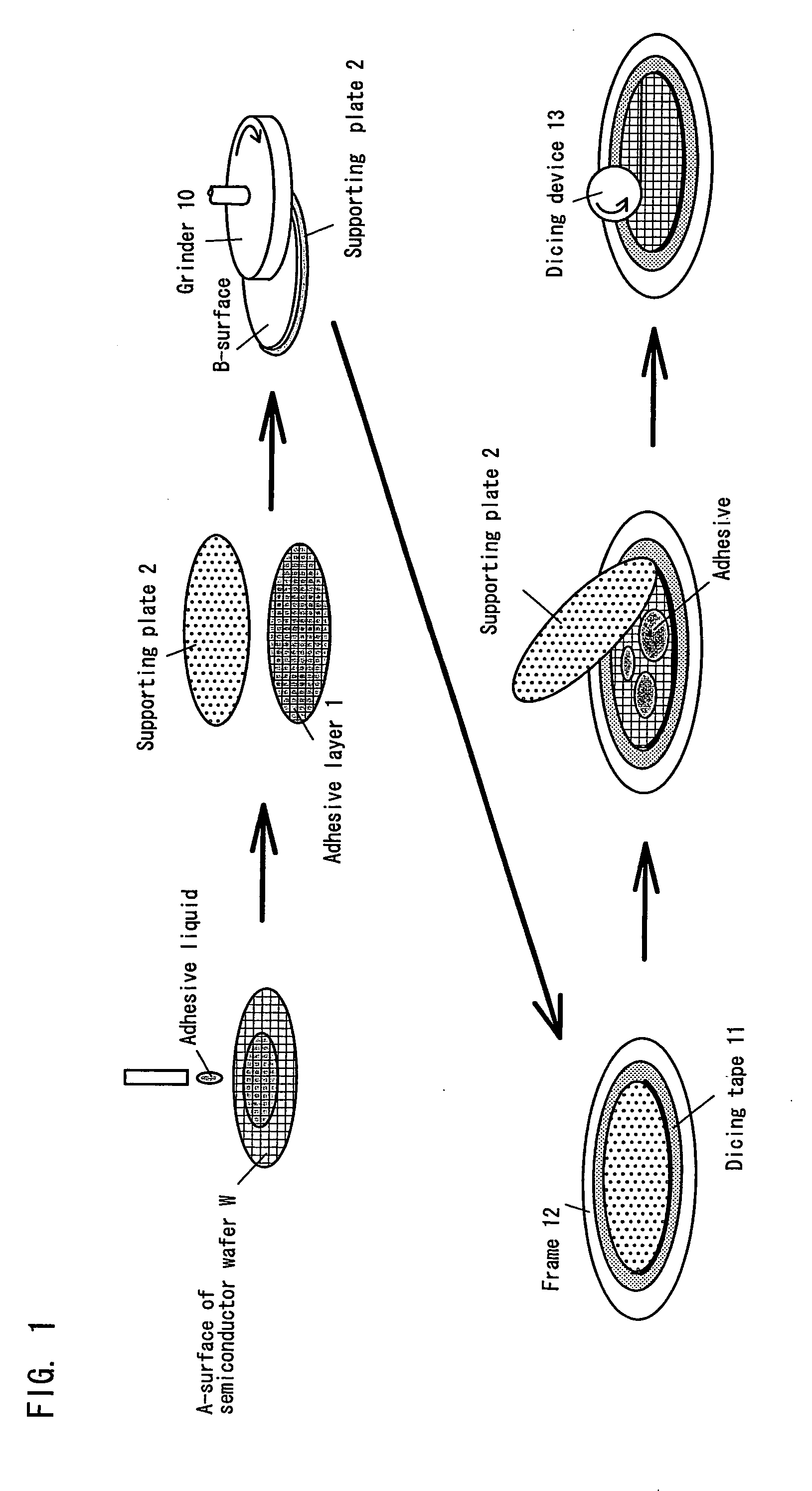
[0028] Embodiments of the present invention will be described below with reference to the attached drawings. FIG. 1 is a view showing processes for thinning a semiconductor wafer in which an attaching method according to the present invention is incorporated. First, an adhesive liquid is applied onto a circuit(element)-formed surface of a semiconductor wafer W. The application is conducted by using a spinner or the like. The material for the adhesive liquid is an acrylic resin or a novolac-type phenol resin.

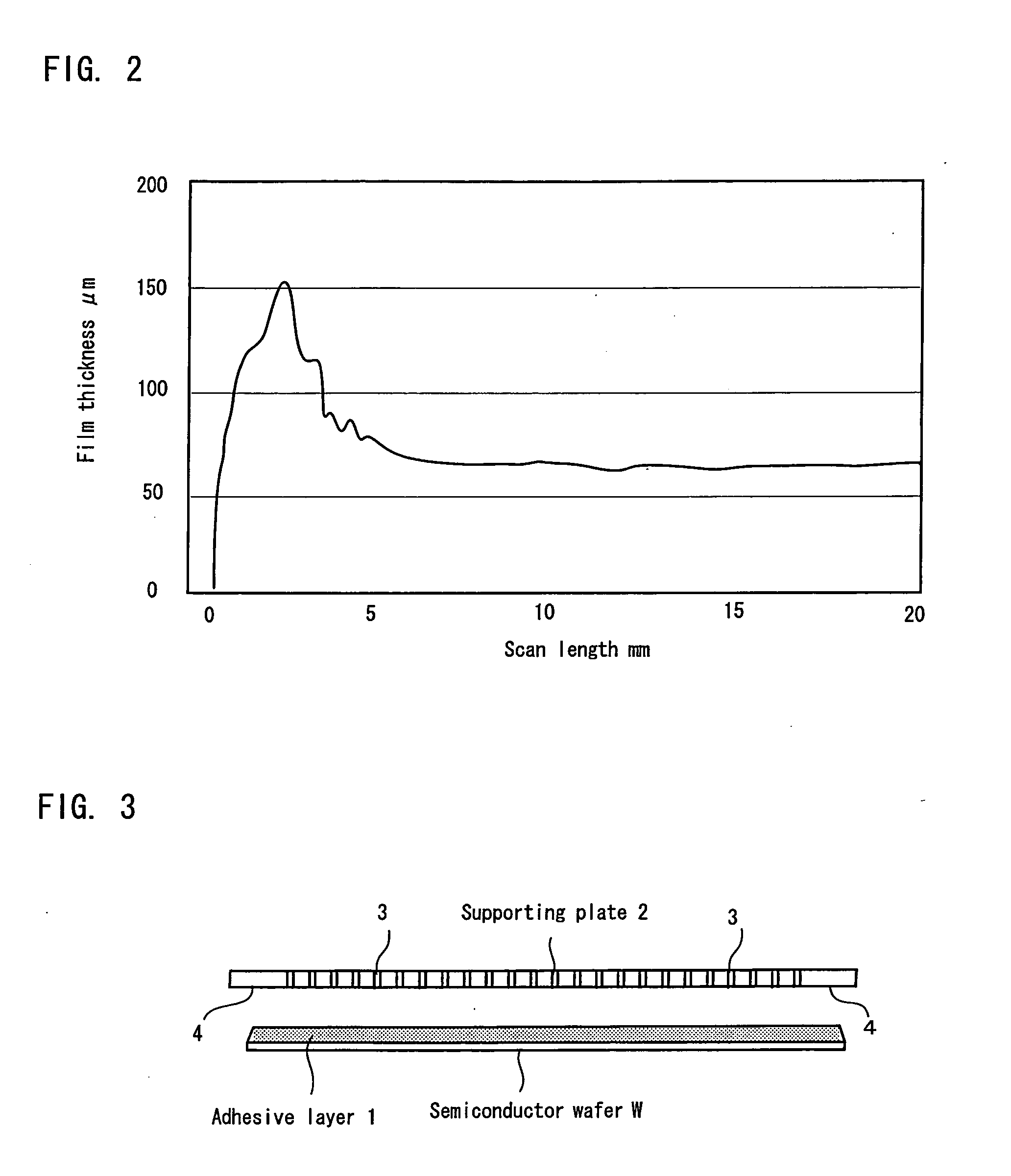
[0029] Next, the adhesive liquid undergoes preliminary drying, so that its flowability is reduced and it can keep its shape as an adhesive layer 1. For the preliminary drying, heating is conducted for 5 minutes at a temperature of 80° C. by using an oven. The thickness of the adhesive layer 1 is determined based on the irregularities of the circuit which has been formed on the surface of the semiconductor wafer W. If a sufficient thickness is not obtained by one application, app...


PUM

PropertyMeasurementUnit
Temperatureaaaaaaaaaa
Thicknessaaaaaaaaaa

Abstract

A method for attaching a substrate such as a semiconductor wafer in which cracking or chipping can be prevented when the substrate is thinned involves applying adhesive liquid onto a circuit (element)-formed surface of a semiconductor wafer. The adhesive liquid undergoes preliminary drying, so that its flowability is reduced and it can keep its shape as an adhesive layer. For the preliminary drying, heating is conducted for 5 minutes at a temperature of 80° C. by using an oven. The thickness of the adhesive layer is determined based on the irregularities of the circuit which has been formed on the surface of the semiconductor wafer. Next, a supporting plate is attached to the semiconductor wafer on which the adhesive layer of a desired thickness has been formed.

Description

BACKGROUND OF THE INVENTION [0001] 1. Field of the Invention [0002] The present invention relates to a method for attaching a substrate such as a semiconductor wafer to a supporting plate when the substrate is thinned by grinding. [0003] 2. Description of the Prior Art [0004] There has been a need of making IC cards or cell phones thinner, smaller, and lighter. In order to satisfy this need, a semiconductor chip to be incorporated therein must be thin. Although the thickness of a wafer which forms a semiconductor chip is 125-150 μm at present, it is expected that the thickness of a semiconductor wafer must be 25-50 μm for a next generation chip. [0005] A conventional method for thinning a semiconductor wafer is shown in FIG. 6. Specifically, a protecting tape is attached to a surface (A-surface) of a semiconductor wafer on which a circuit (element) has been formed. The wafer is turned over, and the rear surface (B-surface) of the semiconductor wafer is ground by a grinder so as to m...

Claims


Application Information

Patent Timeline
IPC IPC(8): C09J133/00C09J161/06H01L21/02C09J5/00H01L21/30H01L21/301H01L21/304H01L21/68H01L21/683H01L21/78
CPCH01L21/6835H01L21/6836H01L21/78Y10T428/28H01L2221/68327H01L2221/6834H01L2221/68318H01L21/304H01L21/02
Inventor MIYANARI, ATSUSHIDOI, KOSUKEMIYAGI, KENINAO, YOSHIHIROMISUMI, KOICHI
Owner NXP BV
Why Eureka
Try Eureka