

Chemically amplified resist composition and method for forming patterned film using same
a technology of amplified resist and composition, which is applied in the direction of photosensitive materials, instruments, photomechanical equipment, etc., can solve the problems of reducing the durability of the lens made of quartz or the like used in the radiation source apparatus, the inability to achieve improvement throughput, and the need for a high laser power, etc., to achieve the elimination of protective groups on the acid-sensitive lens, the effect of improving sensitivity and high reactivity
- Summary
- Abstract
- Description
- Claims
- Application Information
AI Technical Summary
Benefits of technology
Problems solved by technology
Method used
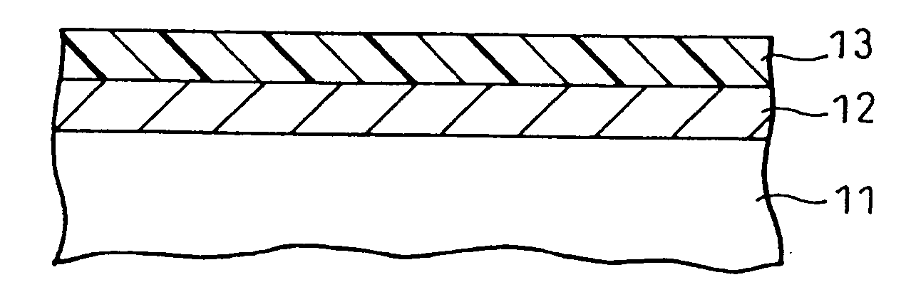
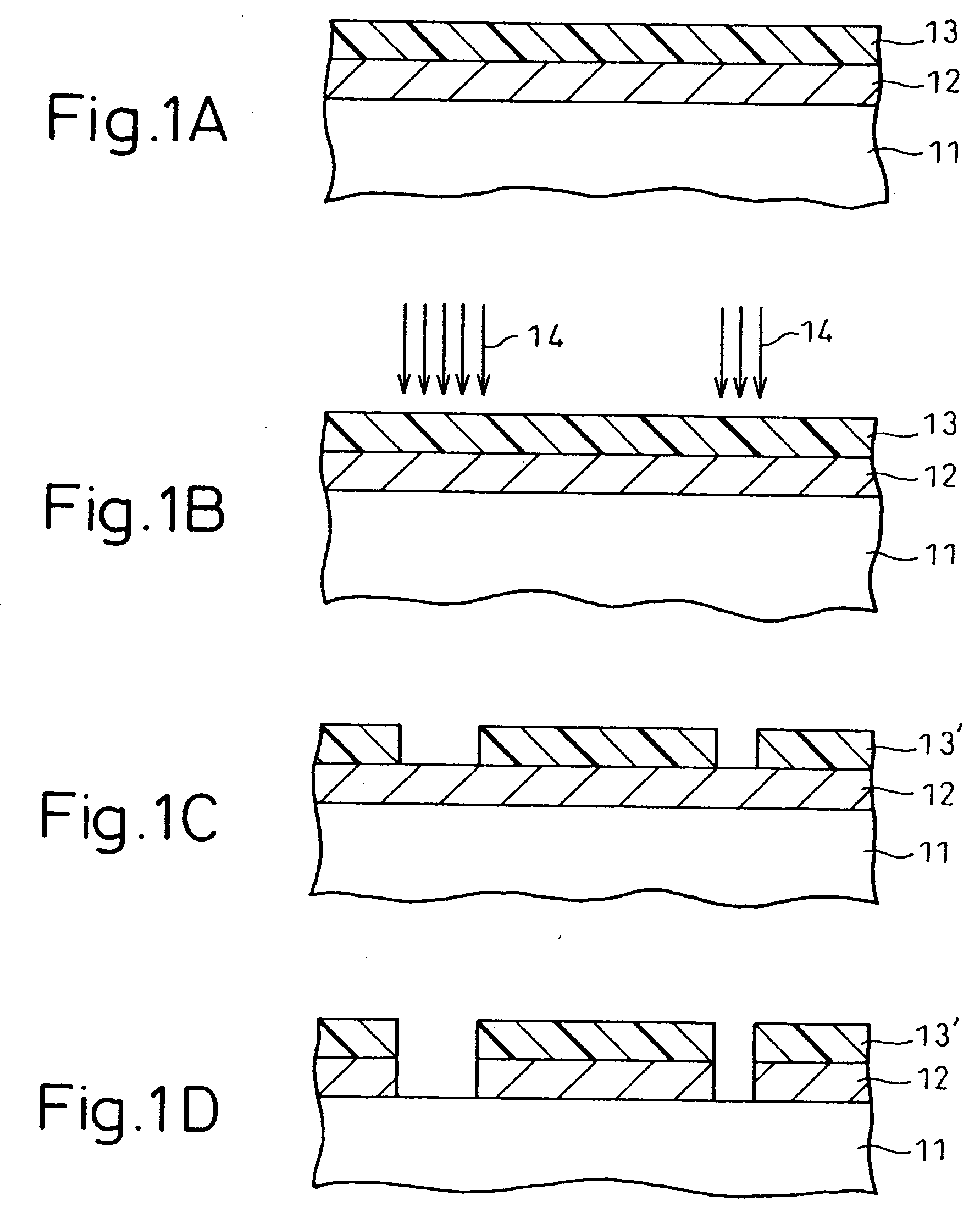
Image

Examples
example 1
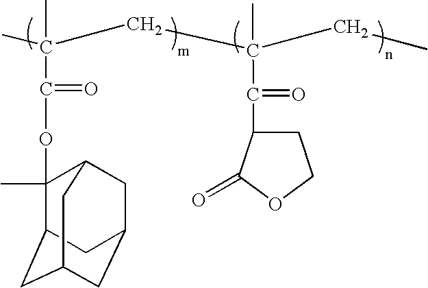
[0034] From two types of metacrylic monomers, 2-methyladamantyl metacrylate and gamma-butyrolactone methacrylate, a copolymer was prepared as described in JP-A-11-12326, the copolymer being represented by the formula:
and having a weight average molecular weight of about 10,000 and an m / n ratio of 50:50. Using the copolymer as a base resin, a positive chemically amplified resist composition was prepared by mixing 100 parts by mass of copolymer, 3 parts by mass of photo acid generator based on an onium salt of sulfonic acid and 0.2 part by mass of aniline-based quencher, the photo acid generator and the quencher being represented by the following formula, respectively:
[0035] The composition thus prepared was then dissolved in 1000 parts by mass of solvent (propylene glycol monomethyl ether acetate (PGMEA)), and two resist solutions were prepared by adding, to the resultant mixture, a compound represented by the formula:
as an additive, in amounts of 5% by mass and 10% by mass, ...
example 2
[0036] Each of the resist solutions prepared in Example 1 was applied to a silicon wafer substrate, and soft-baked at 115° C. for 60 seconds to form a film. The film was then irradiated with an ArF excimer laser beam in exposure energies stepwise increasing from 4 mJ / cm2 at constant intervals of 0.2 mJ / cm2, and was post-exposure baked at 115° C. for 60 seconds to form a resist film having a thickness of 0.4 micrometer. Subsequently, the resist film was developed using a developer of 2.38% TMAH. In consequence, the initial exposure energy of 4 mJ / cm2 was already in excess, and the resist film could not be patterned. Accordingly, a resist solution was prepared again by changing the amount of additive to 1% by mass, and the same procedure was followed. In consequence, it was verified that a 1:1 line-and-space pattern of 130 nanometers could be formed at a high sensitivity of 10 mJ / cm2 or more.
example 3
[0037] Using, as a base resin, a polymeric resin represented by the formula:
which was derived from a polyhydroxystyrene (PHS) commonly used in resists for KrF laser beam (wavelength: 248 nm) exposure by partially substituting hydroxyl with a leaving substituent, the resin having a weight average molecular weight of about 10,000 and an m / n ratio of 70:30, a positive chemically amplified resist solution was prepared by adding, to 100 parts by mass of base resin, the photo acid generator and the quencher used in Example 1, in amounts of 3 parts by mass and 0.2 part by mass, respectively, and further adding the compound used in Example 2, in an amount of 5% by mass. The resultant resist solution was used to carry out a process treatment similar to that described in Example 2 through the exposure using a KrF laser beam. In consequence, it was verified that a 1:1 line-and-space pattern of 130 nanometers could be formed at a high sensitivity of 20 mJ / cm2 or less.
PUM
| Property | Measurement | Unit |
|---|---|---|
| thickness | aaaaa | aaaaa |
| wavelength | aaaaa | aaaaa |
| dry-etching resistance | aaaaa | aaaaa |
Abstract
Description
Claims
Application Information