Nonvolatile semiconductor memory and making method thereof

a semiconductor memory and non-volatile technology, applied in the direction of semiconductor devices, electrical equipment, transistors, etc., can solve the problems of increased wiring resistance of the memory gate electrode, unfavorable wiring resistance, and difficult realization

Inactive Publication Date: 2005-08-11
RENESAS ELECTRONICS CORP
View PDF11 Cites 57 Cited by
  • Summary
  • Abstract
  • Description
  • Claims
  • Application Information

AI Technical Summary

Benefits of technology

[0020] It is therefore an object of the present invention to solve the foregoing problems and provid...

Problems solved by technology

However, since existent memories storing charges in the insulative films are required to conduct charge and discharge of electric charges while possessing sufficient charge retaining characteristics, they are difficult to realize.
However, when the structure is formed by utilizing a usual sidewall spacer, while the gate length can be reduced, this poses a problem in that the wiring resistance of the memory gate electrode is increased.
The problem of the wiring resistance is unfavorable for integrated semiconductor nonvolatile memory cells.
For example, increase of the gate resistance makes the bias supply instable, which gives a significant problem to the high-speed operation of the cell.
As can be seen from the figure, the memory gate w...

Method used


Image

  • Nonvolatile semiconductor memory and making method thereof
  • Nonvolatile semiconductor memory and making method thereof
  • Nonvolatile semiconductor memory and making method thereof

Examples


embodiment 1

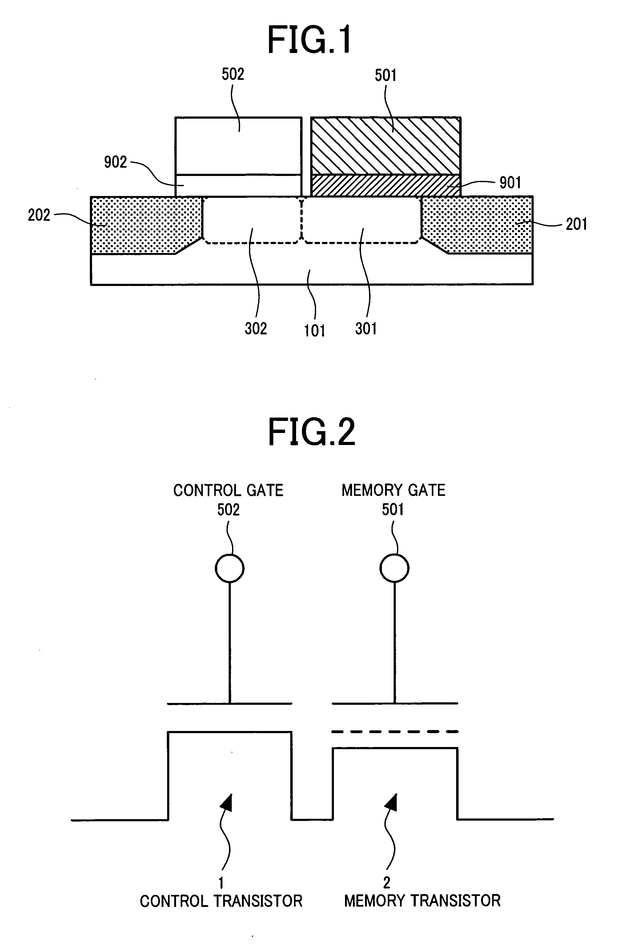
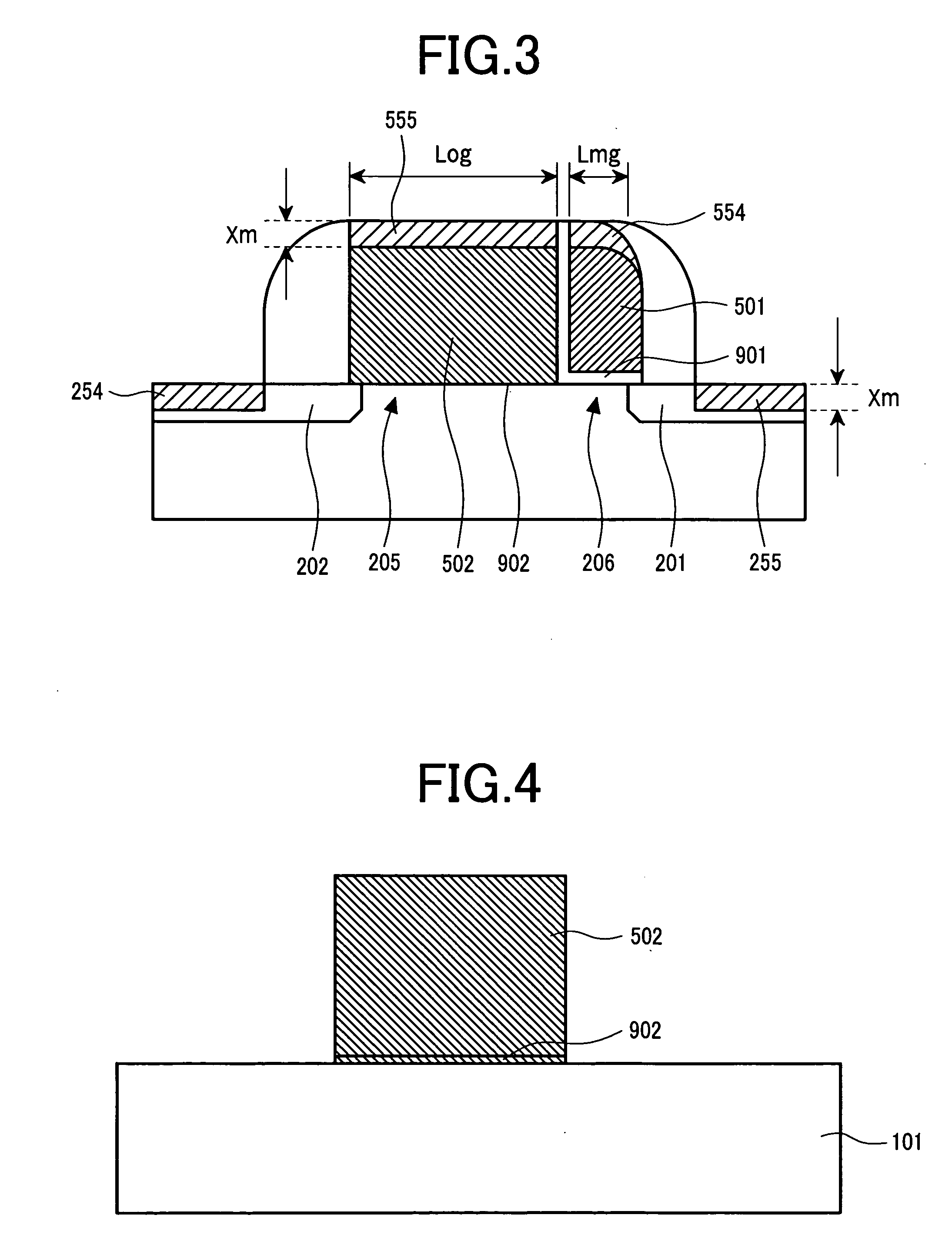
[0071] The present invention is to be described specifically with reference to embodiments thereof. At first, the method of formation and the structure according to the invention are to be described focusing on a memory gate as a principal portion thereof.

[0072] FIGS. 4 to 10 are schematic cross-sectional views of a semiconductor device according to a first embodiment of the invention.

[0073] In accordance with a usual manufacturing method of a semiconductor device, a semiconductor substrate having a well 101 is provided. After formation of a gate oxide film 902 of 3 nm thick in the surface of an active region in the well 101, phosphorus-doped polycrystal silicon is deposited to a thickness of 200 nm by a CVD method. Then, the polycrystal silicon layer is fabricated into a desired shape by using usual lithography to form a selection gate 502 (FIG. 4).

[0074] Then, after formation of a stacked structure 901 of a silicon oxide film, a silicon nitride film and a silicon oxide film as ...

embodiment 2

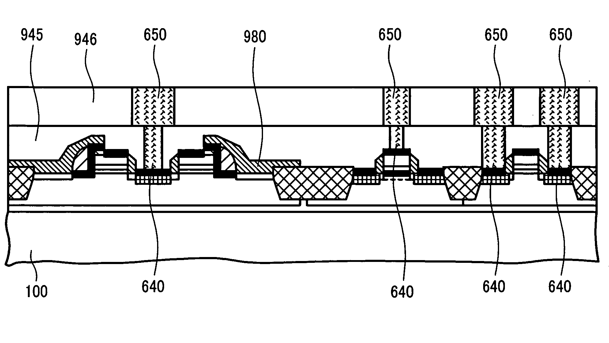
[0085] This embodiment illustrates a manufacturing step for a semiconductor integrated circuit including a memory cell portion and a memory peripheral circuit portion. FIGS. 12 to 23 are schematic cross-sectional views showing a semiconductor device of this embodiment in the order of steps. This embodiment shows the state of forming the memory cell portion and the memory peripheral circuit portion, particularly, a high voltage withstanding device portion and a usual device portion since high voltage withstanding is necessary, for example, in writing.

[0086] In FIG. 12, each of the regions for the memory cell portion (1) and the memory peripheral circuit portion, a high voltage withstanding memory portion (2) requiring a high voltage, particularly, in writing and a usual device portion (3) are depicted each by the reference described above. FIGS. 13 and 14 lack the indications for the regions but the corresponding regions are the same as those in FIG. 12. Further, FIG. 15 depicts mor...


PUM


Abstract

A nonvolatile semiconductor memory device of a split gate structure having a gate of low resistance suitable to the arrangement of a memory cell array is provided. When being formed of a side wall spacer, a memory gate is formed of polycrystal silicon and then replaced with nickel silicide. Thus, its resistance can be lowered with no effect on the silicidation to the selection gate or the diffusion layer.

Description

CLAIM OF PRIORITY [0001] The present application claims priority from Japanese application JP 2004-033297 filed on Feb. 10, 2004, the content of which is hereby incorporated by reference into this application. BACKGROUND OF THE INVENTION [0002] 1. Field of the Invention [0003] The present invention relates to semiconductor memory devices and making methods thereof and it particularly relates to a semiconductor memory device having a nonvolatile memory structure and a making method thereof. [0004] 2. Description of the Related Art [0005] It is a nonvolatile memory that is one of integrated semiconductor memories assembled in a large scale integrated (LSI) device or chip. This is a device that retains memory information even after a power supply for an LSI chip is turned off and this is an extremely important device to use the LSI chip for various applications. [0006] For the nonvolatile semiconductor device, the so-called float gate type memory or a memory using an insulative film is...

Claims


Application Information

Patent Timeline
IPC IPC(8): H01L21/8247H01L21/00H01L21/28H01L21/336H01L21/8242H01L27/105H01L27/115H01L29/788H01L29/792
CPCH01L21/28273H01L27/105H01L27/115H01L29/66825H01L27/11526H01L27/11531H01L27/11521H01L29/40114H10B69/00H10B41/30H10B41/40H10B41/42
Inventor HISAMOTO, DIGHYASUI, KAN
Owner RENESAS ELECTRONICS CORP
Why Eureka
Try Eureka