Polymer compound, resist material and pattern formation method
- Summary
- Abstract
- Description
- Claims
- Application Information
AI Technical Summary
Benefits of technology
Problems solved by technology
Method used
Image
Examples
embodiment 1
[0072] A polymer compound according to Embodiment 1 of the invention will now be described.
[0073] The polymer compound of Embodiment 1 includes a first unit represented by a general formula shown as Chemical Formula 30 below and a second unit represented by a general formula shown as Chemical Formula 31 below. The polymer compound of Embodiment 1 has a weight-average molecular weight not less than 1,000 and not more than 500,000 and preferably not less than 2,000 and not more than 100,000.
[0074] In Chemical Formulas 30 and 31, R1, R2 and R3 are the same or different and are a hydrogen atom, a fluorine atom, or a straight-chain alkyl group, a branched or cyclic alkyl group or a fluoridated alkyl group with a carbon number not less than 1 and not more than 20; R5 and R6 are the same or different and are a hydrogen atom, a straight-chain alkyl group, a branched or cyclic alkyl group or a fluoridated alkyl group with a carbon number not less than 1 and not more than 20, or a protecti...
embodiment 5
[0124] A pattern formation method according to Embodiment 5 of the invention will now be described.
[0125] In the pattern formation method of Embodiment 5, the resist material according to Embodiment 3 or 4 is used, and the pattern formation method includes the following procedures:
[0126] First, the resist material according to Embodiment 3 or 4 is applied on a substrate such as a silicon wafer in a thickness of 0.1 through 1.0 pm by spin coating or the like. Thereafter, the resultant substrate is subjected to pre-bake by using a hot plate at a temperature of 60 through 200° C. for 10 seconds through 10 minutes and preferably at a temperature of 80 through 150° C. for 30 seconds through 5 minutes. Thus, a resist film is formed.
[0127] Next, the resist film is irradiated through a photomask having a desired pattern with high energy beams such as deep UV, excimer laser or X-rays, or electron beams at exposure of approximately 1 through 200 mJ / cm2 and preferably approximately 10 throu...
example 1
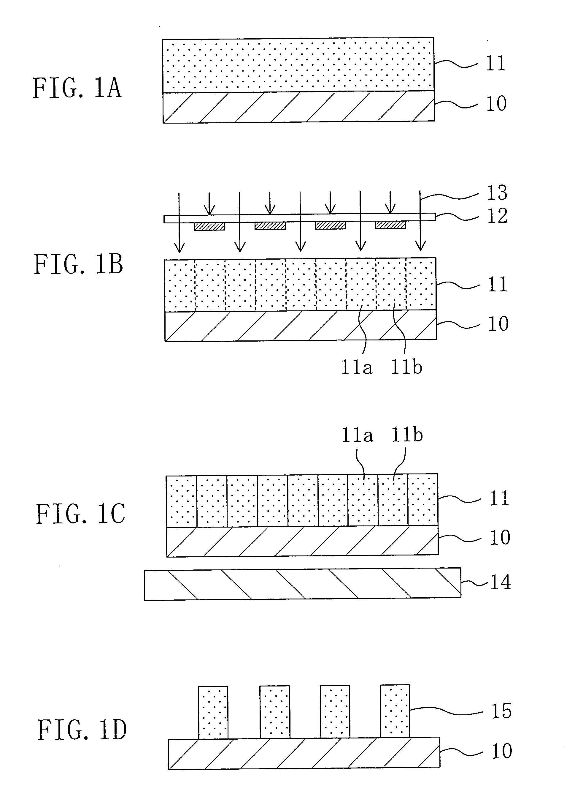
[0132] Example 1 for embodying the chemically amplified resist material of Embodiment 4 and the pattern formation method of Embodiment 5 will now be described with reference to FIGS. 1A through 1D.
[0133] First, a chemically amplified resist material having the following composition is prepared:
[0134] Base polymer: polymer in which a first unit represented by Chemical Formula 45 and a second unit represented by Chemical Formula 46 are polymerized Acid generator: triphenylsulfonium nonaflate (4 wt% based on the base polymer) Solvent: propylene glycol monomethyl ether acetate
[0135] Next, as shown in FIG. 1A, the chemically amplified resist material having the above-described composition is applied on a semiconductor substrate 10 by spin coating, thereby forming a resist film 11 with a thickness of 0.2 μm. At this point, since the base polymer is alkali-insoluble, the resist film 11 is alkali-insoluble.
[0136] Next, as shown in FIG. 1B, the resist film 11 is subjected to pattern exp...
PUM
| Property | Measurement | Unit |
|---|---|---|
| Nanoscale particle size | aaaaa | aaaaa |
| Nanoscale particle size | aaaaa | aaaaa |
| Nanoscale particle size | aaaaa | aaaaa |
Abstract
Description
Claims
Application Information


