
Nitride based semiconductor laser diode device with a bar mask

a semiconductor laser and diode device technology, applied in the direction of semiconductor lasers, semiconductor laser structure details, active medium materials, etc., can solve the problems of poor device function, cracking of epitaxial layer, and even severe damage, so as to reduce the occurrence of cracks and increase the thickness of epitaxial layer

Active Publication Date: 2005-09-15
NAT CHUNG SHAN INST SCI & TECH
View PDF2 Cites 54 Cited by
  • Summary
  • Abstract
  • Description
  • Claims
  • Application Information

AI Technical Summary

Benefits of technology

[0011] The invention provides an epitaxial growing structure, which uses a specific mechanism for the surface, so as to increase the thickness of the epitaxial layer in the gallium nitride laser diode structure but reduce the occurrence of crack.

Problems solved by technology

When the thickness of the epitaxial layer is greater than a certain critical value, the material then release the energy by a crack form, resulting in a crack of the epitaxial layer.
If the thickness of the epitaxial layer is too large, a poor function of the device or even a severe damage would occur due to the crack.
However, if the thickness of the epitaxial layer is not sufficient large, a poor performance may also occur.
The foregoing technology can only be used for solving the strain energy or effect, which are caused by epitaxial layer between substrate and the gallium nitride, or inside the device.
Taking the gallium nitride laser diode as an example, the application for the foregoing conventional technologies is basically limited to the epitaxial layer under the active layer.
The epitaxial layer above the active layer still has the problem of hetero material structure.
In other words, the conventional method still cannot effectively solve the problem of crack in the epitaxial layer above the active layer.
However, these kinds of technologies for reducing the strain and the defects is not effective with respect to strain energy existing in the surface hetero epitaxial layer. FIG. 2, is a picture, schematically illustrating the crack occurring on the surface of the epitaxial layer for the conventional gallium nitride laser diode structure.
If the Alx Ga1-x N layer is too thick, the crack is then easily occurring, and causes a failure of device.
However, if the cladding layer is not sufficiently thick, the effect of light confinement then is getting worse, and the performance of device is then poor.
Thus, it is a difficult issue for fabrication that how to control the thickness of epitaxial layer and the composition, so as to reduce the cracking of the epitaxial layer and improve the performance of the device.

Method used


Image

  • Nitride based semiconductor laser diode device with a bar mask
  • Nitride based semiconductor laser diode device with a bar mask
  • Nitride based semiconductor laser diode device with a bar mask

Examples


embodiment 1

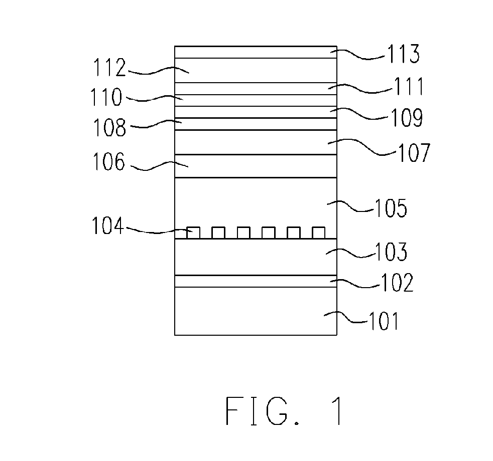
[0024]FIG. 3 is a cross-sectional view, schematically illustrating the structure of a gallium nitride laser diode, according to the first preferred embodiment of this invention. A substrate 301 is provided. The substrate 301 includes, for example, sapphire (Al2O3), silicon carbide (SiC), gallium nitride (GaN), Spinel (MgAl2O4), gallium arsenide (GaAs), zinc oxide (ZnO), silicon (Si), and so on. A gallium nitride compound semiconductor buffer layer 302 is formed on substrate 301 with an amorphous and / or polycrystallized structure and a thickness of 50-500 Angstrom. An N-type GNCS 303 is formed on the buffer layer 302 with a thickness of about 3-7 microns.

[0025] After the crystal growth, the whole structure is shifted out from the crystal growing machine, and the coating, photolithography and etching processes are performed to form a lower bar mask substance 304 on the N-type GNCS layer 303. The direction of the bar can be any direction. The thickness can be, for example, 100-2000 An...

embodiment 2

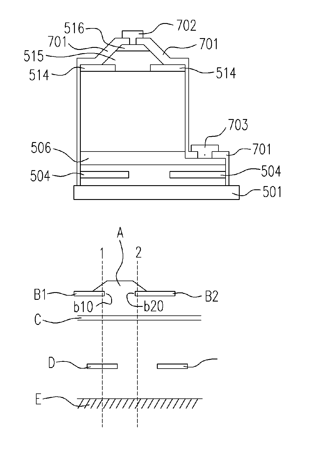
[0030]FIG. 5 is a cross-sectional view, schematically illustrating the structure of a gallium nitride laser diode, which includes a substrate 501 having the materials including aluminum oxide, silicon carbide, gallium nitride, Spinel, gallium arsenide, zinc oxide, silicon, and so on. A GNCS buffer layer 502 is formed on the substrate 501 as an amorphous and / or polycrystallized structure by a thickness of 50-500 Angstroms. An N-type GNCS layer 503 is formed on the GNCS buffer layer 502 by a thickness of about 3-7 microns.

[0031] After the crystal growth, the whole structure is shifted out from the crystal growing machine, and the coating, photolithography and etching processes are performed to form a lower bar mask substance 504 on the N-type GNCS layer 503. The features of the lower bar mask substance 504 is similar to the lower bar mask substance 304 in Embodiment 1. Each bar of the lower bar mask substance 504 has a cross-sectional shape in rectangular or any shape with similar fu...

embodiment 3

[0035]FIG. 6 is a cross-sectional view, schematically illustrating the structure of a gallium nitride laser diode, according to the third preferred embodiment of this invention. The structure is formed by photolithography, etching, and coating processes on the structure of gallium nitride laser diode (see FIG. 3) in Embodiment 1. In addition to the gallium nitride laser diode in epitaxial structure, the structure further includes an insulating layer 601 from, for example, silicon oxide. A P-type metal electrode 602 is formed on the P-type metal electrode contact layer 315. An N-type electrode 603 is formed on the heavily doped N-type GNCS layer 306.


PUM


Abstract

A nitride based semiconductor laser diode device comprising a selective growth mask with a grating structure is proposed. The island-like stacked epitaxial layers including the P-type cladding layer is formed from the selective growth mask upon the active layer of the semiconductor laser structure. This proposed structure can reduce the strain by the deformation due to the isolate structure. Thus, increase of thickness of the cladding layer and / or increase of composition difference can be achieved without crack existing in the island-like stacked epitaxial layers. The optical confinement can be effectively improved.

Description

CROSS-REFERENCE TO RELATED APPLICATION [0001] This application is a divisional of a prior application Ser. No. 10 / 250,200, filed Jun. 12, 2003, which claims the priority benefit of Taiwan application serial no. 91121531, filed on Sep. 20, 2002. All disclosure of the Taiwan application is incorporated herein by reference.BACKGROUND OF THE INVENTION [0002] 1. Field of Invention [0003] The present invention relates to a semiconductor device by gallium nitride compound. More particularly, the present invention relates to a structure capable of applying on a gallium nitride laser diode device for increasing a thickness of a surface epitaxial layer. In the specification, the surface epitaxial layer is referring to a patterned epitaxial layer in the gallium nitride laser diode device. [0004] 2. Description of Related Art [0005] The typical optoelectronics device is a hetero structure. Since the crystal structure between the hetero epitaxial layers is not matched and the thermal expansion c...

Claims


Application Information

Patent Timeline
Patent Type & Authority Applications(United States)
IPC IPC(8): H01L21/00H01S5/00H01S5/02H01S5/32H01S5/323
CPCH01S5/0213H01S5/0218H01S2304/12H01S5/3211H01S5/32341H01S5/3201
Inventor LAN, WEN-HOWSHIANG, YUH-DERLIN, JIA-CHINGLIN, KER-JUNPERNG, KAI-FUNGCHERNG, YA-TUNG
Owner NAT CHUNG SHAN INST SCI & TECH
Features
  • Generate Ideas
  • Intellectual Property
  • Life Sciences
  • Materials
  • Tech Scout
  • Unparalleled Data Quality
  • Higher Quality Content
  • 60% Fewer Hallucinations
Learn More