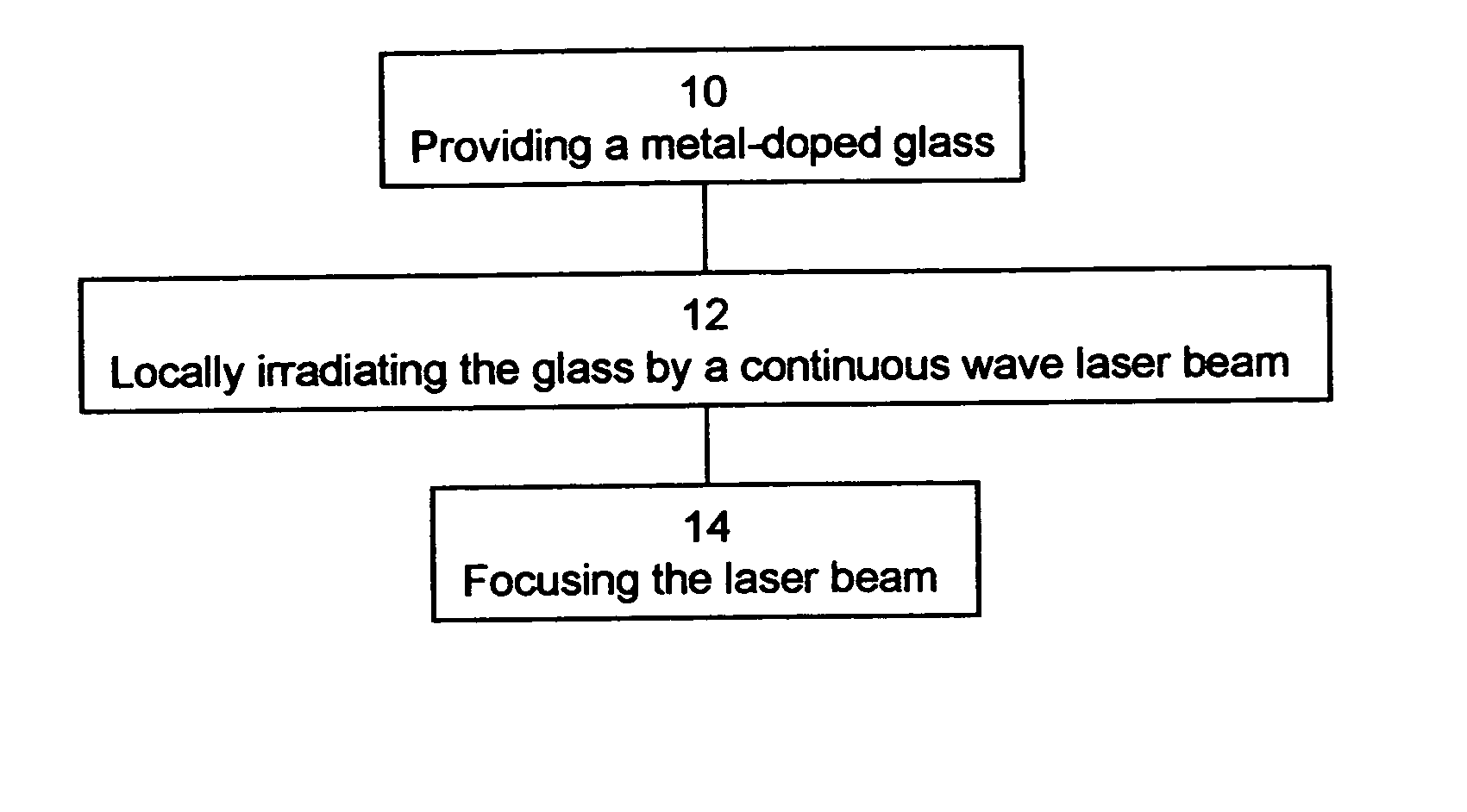
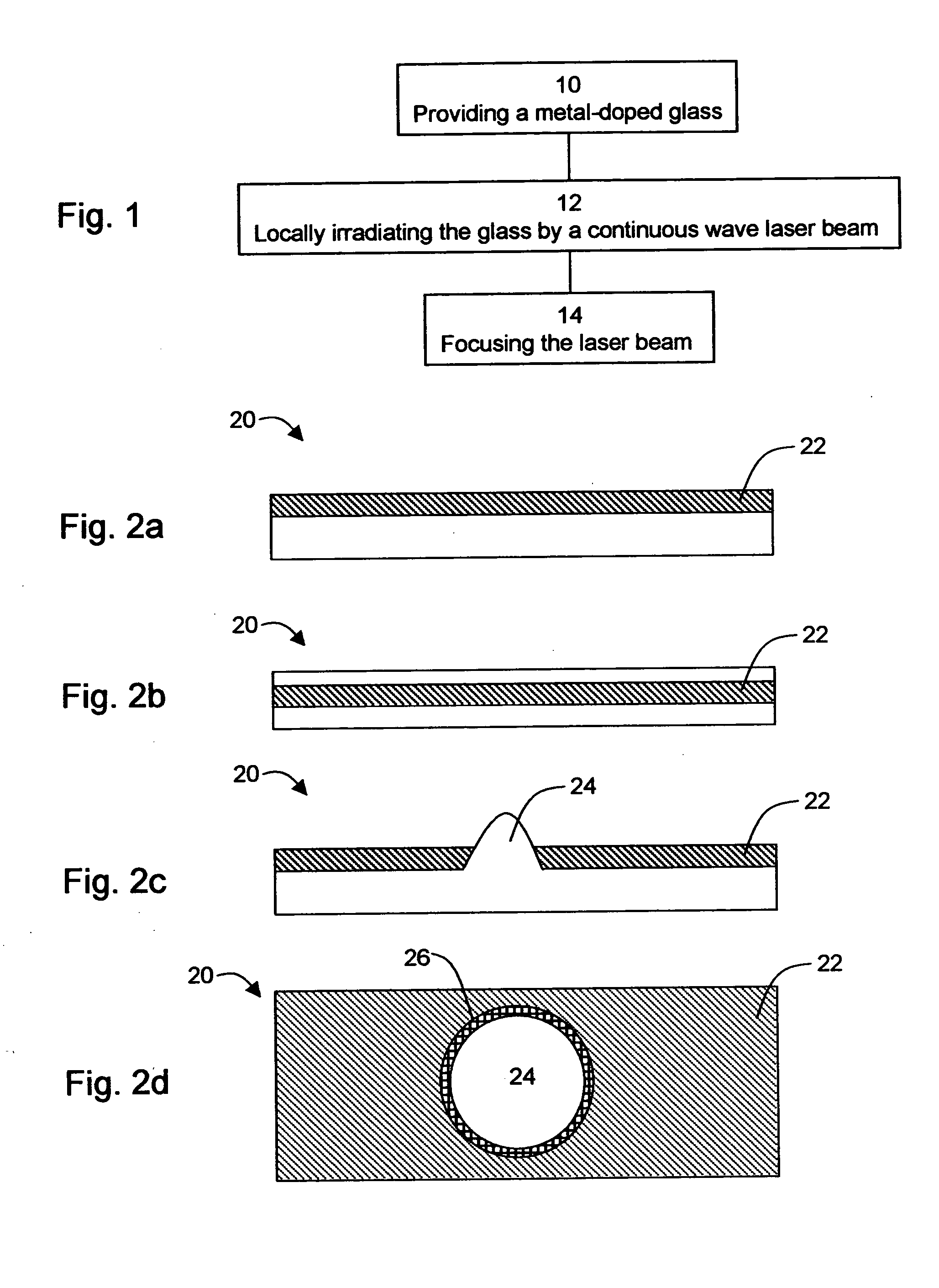
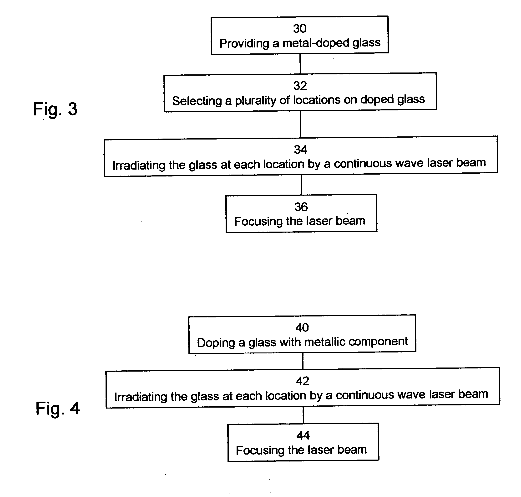
Microlens and method of marking same
a technology of microlens and markings, applied in the field of microoptical elements, can solve the problems of difficult control of the resist flow process of the microlens, loss of more than two-thirds of the luminous flux through the lcd panel, and difficulty in creating arrays of microlenses with the same curvature and dimensions
- Summary
- Abstract
- Description
- Claims
- Application Information
AI Technical Summary
Benefits of technology
Problems solved by technology
Method used
Image

Examples
example 1
Microlens Formation
[0207] Experimental
[0208] Experiments were performed, in accordance with the teachings of present invention described above, on several glass samples with embedded silver (Ag) clusters of 20 nm diameter and average bulk density of 1.3·1016 cm3. The preparation of the glass / Ag composite consisted of two stages: (i) doping of the subsurface layer of the glass with Ag+ ions; and (ii) growing silver clusters within this layer in a Hydrogen atmosphere. The glass matrix was earlier developed for ion-exchange applications, and its composition is presented in Table 1, below.
TABLE 1OxideSiO2Al2O3B2O3ZrO2As2O3Na2OLi2Omol. %60.06.010.03.70.119.70.5
[0209] For the first stage, a conventional technique of ion exchange was used to exchange sodium ions of the glass with silver ions, in a mixture of 5 mol. % of AgNO3 and 95 mol. % of NaNO3 melts, at a working temperature of about 340° C.
[0210] The processing led to decreasing Na+ ion concentration and to increasing Ag+ concen...
example 2
Calculation of the Temperature Distribution
[0226] This Example is intended to exemplify the procedure of predicting the lens radius and height as functions of the laser power P, by calculating the temperature distribution around the “hot spot” inside the glass.
[0227] Analytical Calculation
[0228] A small volume of the glass, restricted by a “boundary” isotherm, Ts, which is higher than the glass transition temperature, is characterized during irradiation by a decreased viscous relaxation time (of the order of seconds). A circle of radius R at the glass surface corresponding to this isotherm defines the radius of the microlens. The height of the microlens, h, is determined from the depth of the liquid “drop”, H, and the temperature distribution in the z-direction.
[0229] For a laser intensity distribution, I(r,z), where r is the radial distance from the center of the beam, and α(z-dependent) absorption coefficient, α(z), of the doped glass, the steady state form of the diffusion eq...
PUM
| Property | Measurement | Unit |
|---|---|---|
| Fraction | aaaaa | aaaaa |
| Percent by mass | aaaaa | aaaaa |
| Length | aaaaa | aaaaa |
Abstract
Description
Claims
Application Information