Nitride semiconductor laser device and nitride semiconductor device

a laser device and semiconductor technology, applied in semiconductor lasers, semiconductor laser structural details, war-like protection, etc., can solve the problems of increased threshold current, uneven distribution of impurities and the like within the laser device, uneven composition of indium, etc., to improve the working life and device characteristics.

Active Publication Date: 2005-10-13
NICHIA CORP
View PDF9 Cites 85 Cited by
  • Summary
  • Abstract
  • Description
  • Claims
  • Application Information

AI Technical Summary

Benefits of technology

[0010] The present invention addresses the issues described above, and therefore an object of the present invention is to provide a device wherein the nitride semiconductor layer has uniform compositional distribution; for example, having uniform crystalline characteristics and indium content in the active layer, and thus having improved working life and device characteristics over a broad range of wavelengths.
[0017] By virtue of the device of the present invention, because the principal face of the nitride semiconductor substrate has an off angle in a predetermined direction, it is possible to achieve uniform compositional distribution in the nitride semiconductor layer, for example, in terms of crystalline characteristics and indium content in the active layer. This is because it is possible to achieve flat crystal growth, beginning with surface irregularities in the atomic plane. Consequently, the interface with the semiconductor layer grown on the principal face of the substrate has reduced recessed or protruding height-differential surface irregularities, allowing for more uniform compositional distribution in an active layer capable of achieving emission wavelengths in a range extending from the ultraviolet region of 365 nm or less to a long wavelength region of 500 nm or more. Moreover, it is possible to produce devices having excellent useful life and device characteristics in this broad wavelength band.
[0018] Furthermore, if the refractive indexes of predetermined semiconductor layers in the device of the present invention have a predetermined relationship, it is possible to suitably adjust the region in which the light generated in the active layer is present, so as to achieve stable optical confinement and thus improve COD level. In addition, it is possible to reduce the spread angle of the light intensity distribution in the perpendicular direction, and to optimize or reduce the aspect ratio to 2 or less. Consequently, it is possible to prevent increases in the threshold voltage due to optical leakage and to produce a highly reliable device with increased optical output efficiency and good convergence.

Problems solved by technology

However, the broad ranges proposed for the size and direction of this off angle for the nitride semiconductor substrate resulted in an uneven composition in indium, aluminum and the like, and an uneven distribution of impurities and the like within the laser device.
In particular, in the case of laser devices comprising an active layer containing indium, depending on the emission wavelength, this may lead to increases in the threshold current.
Nitride semiconductor laser devices are theoretically capable of laser emission over a broad range of wavelengths; in practice however, if compositional distribution, such as the distribution of indium in the active layer, is not uniform, problems arise such as the inability to achieve this broad emission range.
Furthermore, when preparing substrates having large diameters of greater than one inch, as pits and grooves remain on the principal face of the substrate, there are problems in that it is necessary to flatten the surface produced by forming the nitride semiconductor layer on the substrate.

Method used


Image

  • Nitride semiconductor laser device and nitride semiconductor device
  • Nitride semiconductor laser device and nitride semiconductor device
  • Nitride semiconductor laser device and nitride semiconductor device

Examples


embodiment 1

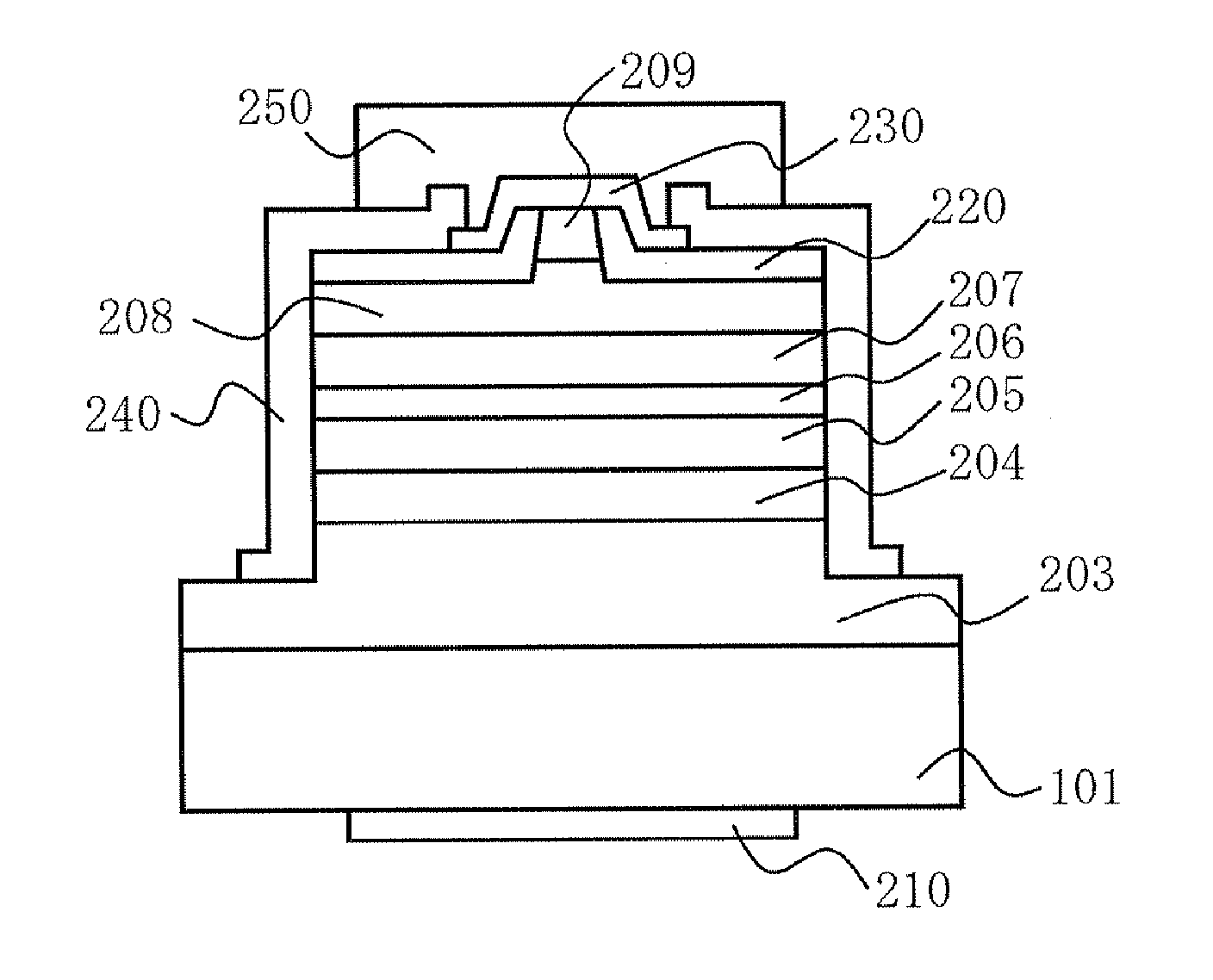
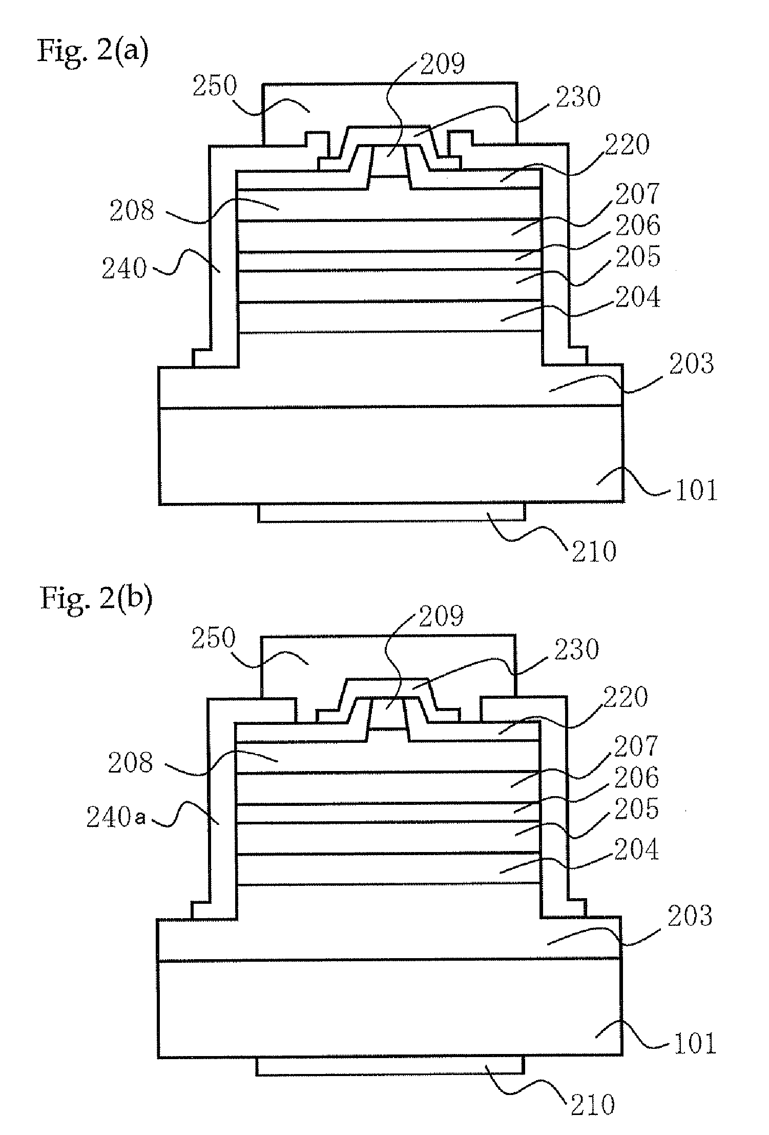
[0122] The structure of the semiconductor laser device according to the present embodiment is shown in FIG. 1(b) and FIG. 2(a).

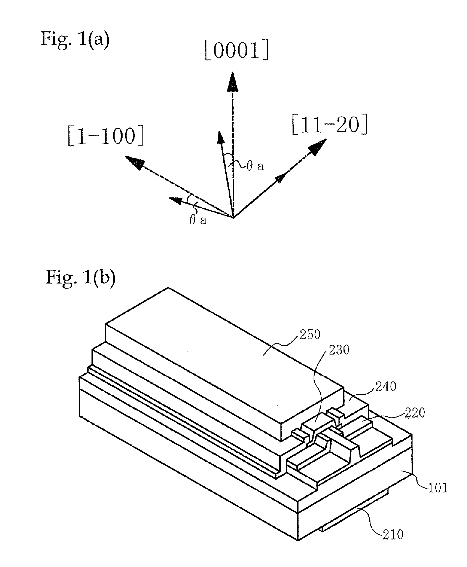
[0123] This laser device comprises, on a GaN substrate 101 with a principal face having an off angle of 0.3° with regard to the (0001) plane and a dislocation density of no greater than 1×10⁶ / cm2, an n-side cladding layer 203, a n-side optical guide layer 204, an active layer 205, a p-side cap layer 206, a p-side optical guide layer 207, a p-side cladding layer 208, and a p-side contact layer 209 are built up in that order with a low temperature buffer layer (not shown in the drawing) and intermediate layer (not shown in the drawing) therebetween.

[0124] A stripe ridge is formed on the p-side contact layer 209 surface and the surface of the p-side cladding layer 208 is exposed on both sides of the ridge.

[0125] An embedding film 220 is formed on the exposed face of the p-side cladding layer 208 and the sides of the ridge.

[0126] A p-electrode 230 is formed ...

embodiment 2

[0165] A laser device was fabricated, which was substantially the same as that in Embodiment 1, with the exception of the changes in the composition thereof shown in the following table.

TABLE 1p-side cladding layerMg doped Al0.1Ga0.9N (0.5 μm)p-side optical guide layerundoped GaN (0.2 μm)active layerSi doped In0.1Ga0.9N barrier layer (700angstrom) and undoped In0.2Ga0.8N welllayer (30 angstrom);GaN barrier layer (700 angstrom)n-side optical guide layerundoped GaN (0.2 μm)n-side cladding layerSi doped Al0.1Ga0.9N (1 μm)

[0166] Laser emission was performed with the resulting devices in the same manner as in Embodiment 1.

[0167] Good continuous emission was observed at room temperature, at emission wavelengths of 460 to 480 nm and a threshold current density of 2.0 kA / cm2.

[0168] Furthermore, there was no cleavage damage to the cavity ends, and with an optical output of CW 80 mW and an operating temperature of 60° C., the life was 3000 hours, meaning that it was possible to fabricate ...

embodiment 3

[0169] The GaN substrate used in this embodiment had the C plane (0001) as the principal plane, and was inclined at an off angle a of 0.23° in the perpendicular direction and at an off angle b of 0.06° in the parallel direction, with respect to the M plane (1-100).

[0170] Furthermore, on the first and second principal faces of the GaN substrate, a first region (1st) comprising the C plane (0001) and a second region (2nd) comprising the (000-1) plane, are formed with widths of 400 μm and 20 μm, respectively. Furthermore, the laser device of this embodiment has the constitution shown in the following table. In other respects, the laser device is substantially the same as that of Embodiment 1.

TABLE 2p-side cladding layersuperlattice layer (total film thickness0.45 μm): undoped Al0.10Ga0.90N (25angstrom) and Mg doped GaN (25 angstrom)p-side optical guide layerundoped GaN (0.125 μm)n-side optical guide layerundoped GaN (0.19 μm)

[0171] Laser oscillation was performed with the resulting ...


PUM


Abstract

A nitride semiconductor laser device comprises, on a principle face of a nitride semiconductor substrate: a nitride semiconductor layer having a first conductivity type; an active layer comprising indium, and a nitride semiconductor layer having a second conductivity type that is different from said first conductivity type, and on the surface of which is formed a stripe ridge; said principal face of said nitride semiconductor substrate having an off angle a (θa) with respect to a reference crystal plane, in at least a direction substantially parallel to said stripe ridge.

Description

BACKGROUND OF THE INVENTION [0001] 1. Field of the Invention [0002] The present invention relates to nitride semiconductor devices comprising an active layer containing indium such as nitride semiconductor laser devices and laser diodes, light emitting diodes (LEDs), photodetectors, high-frequency transistors, and high-voltage transistors. More specifically, it relates to nitride semiconductor lasers and nitride semiconductor devices having improved device characteristics as the result of using a nitride semiconductor substrate having a specific off angle. [0003] 2. Background Information [0004] Laser devices comprising nitride semiconductors such as GaN semiconductors can be used at emission wavelengths ranging from the ultraviolet region of 370 nm or less to wavelengths in the region of 500 nm or more. Substrates on which such laser devices are formed are grown using a lateral growth technique known as Epitaxial Lateral Overgrowth (ELO). [0005] This is a technique wherein GaN is g...

Claims


Application Information

Patent Timeline
Patent Type & Authority Applications(United States)
IPC IPC(8): H01S5/02H01S5/026H01S5/028H01S5/042H01S5/10H01S5/20H01S5/22H01S5/223H01S5/30H01S5/32H01S5/323H01S5/343
CPCB82Y20/00H01S5/0202H01S5/026H01S5/028H01S5/0425H01S5/1082H01S5/2009H01S5/2201H01S5/2214H01S5/2231H01S5/305H01S5/3054H01S5/3202H01S5/34333H01S2304/04H01S2304/12H01S5/320275H01S5/04252H01S5/04254H01S2301/176H01S5/0021E06B7/32E06B5/11
Inventor MATSUYAMA, YUJISUZUKI, SHINJIISE, KOUSUKEMICHIUE, ATSUOYONEDA, AKINORI
Owner NICHIA CORP
Why Eureka
Try Eureka