

Method for producing a coplanar waveguide system on a substrate, and a component for the transmission of electromagnetic waves fabricated in accordance with such a method
- Summary
- Abstract
- Description
- Claims
- Application Information
AI Technical Summary
Benefits of technology
Problems solved by technology
Method used
Image

Examples
first embodiment
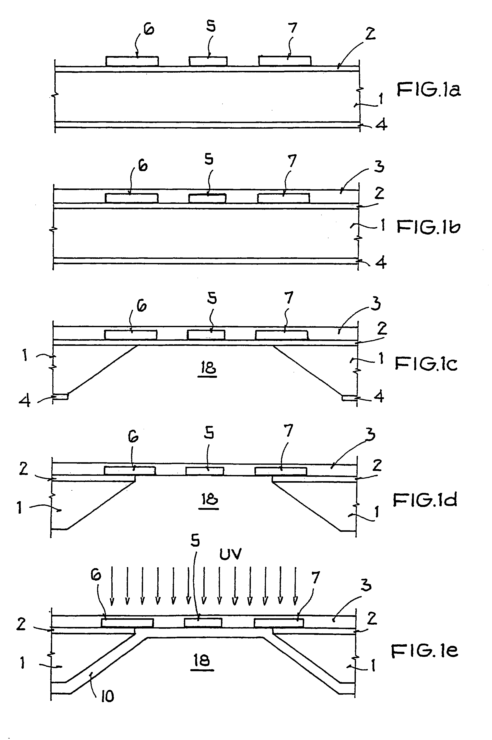
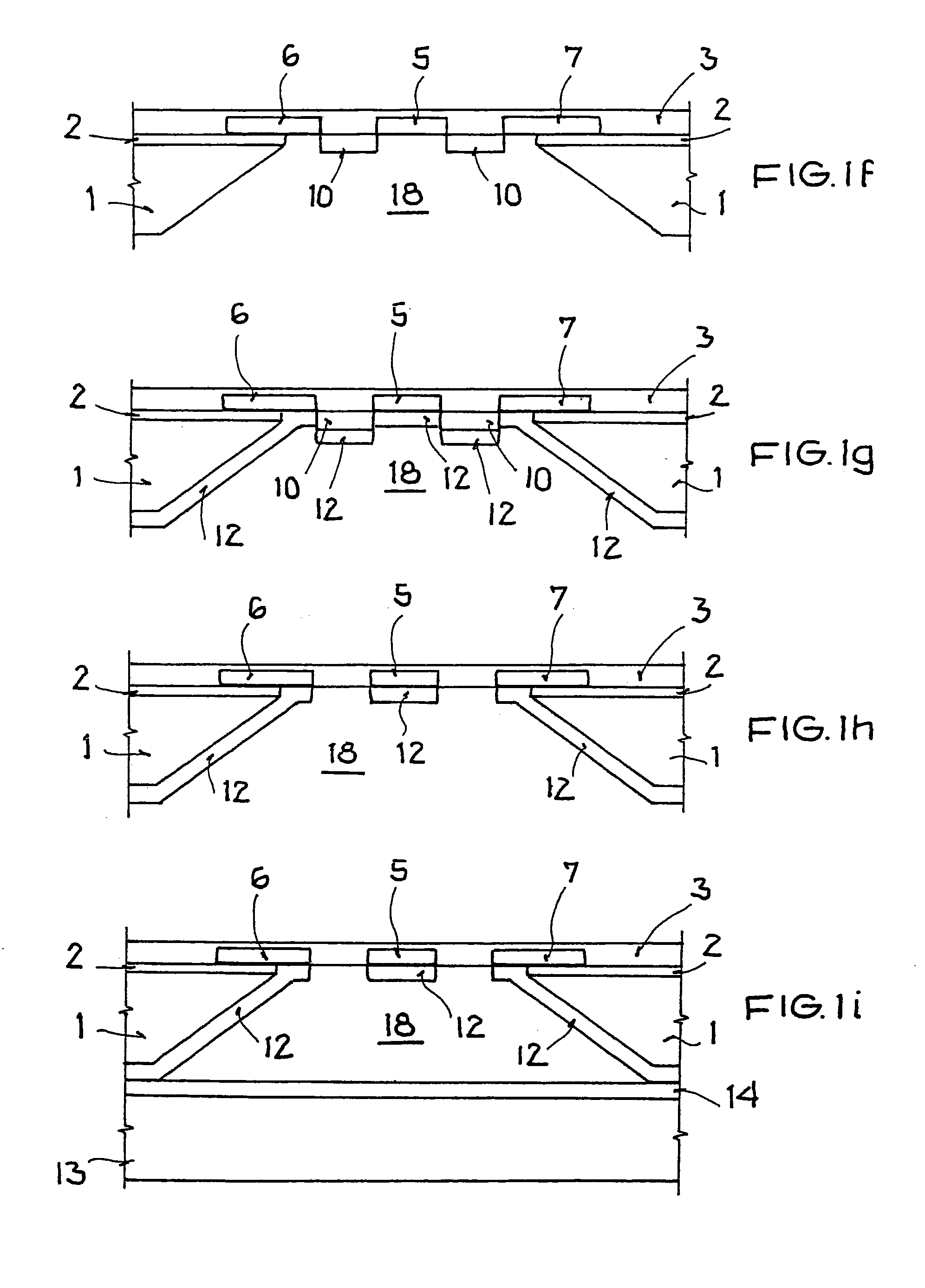
[0042]FIGS. 1a to 1i illustrate cross-sectional views of a component in individual method stages, whereby in FIGS. 1a to 1i, the production method of a component for the transmission of electromagnetic waves according to the present invention is described in detail.
[0043] As is shown in FIG. 1a, in a known method step for producing a finite ground coplanar wave guide (FGCPW), for example, the top side and the bottom side of a substrate 1 are provided with a first dielectric insulating layer 2, that is, with an additional dielectric insulating layer 4 (henceforth referred to as third insulation layer 4), which in certain instances can also be omitted. The substrate 1 is, for example, a low-resistance silicon semiconductor substrate, or the like. The first and third dielectric insulating layer 2, or 4, can be formed as an approximately 1-2 μm-thick silicon nitride or silicon dioxide layer, for example. Subsequently, a signal conductor 5 and two grounding conductors 6 and 7 are metalli...
second embodiment
[0059] Due to the anisotropic back-etching of the substrate 1, as previously described, the oblique-shaped boundary area of the back-etched area 18 is formed. Therebelow, with reference to FIGS. 2a to 2k, a production method according to the present invention is described, whereby the geometric limitations based on the diagonally back-etched areas 18 are reduced and adjacent coplanar waveguide systems can be arranged in closer proximity to one another without diminishing the mechanical stability of the component. With the below-described method, shielding hollow cavities with a higher integration density can be formed below the coplanar waveguide system without adding mechanical instability to the surface of the component.
[0060] As can be seen in FIG. 2a, analogous to the first embodiment in a method step for the production of a finite ground coplanar waveguide (FGCPW), for example, a substrate 1 is provided on its top and bottom sides with a first dielectric insulating layer 2, tha...
fifth embodiment
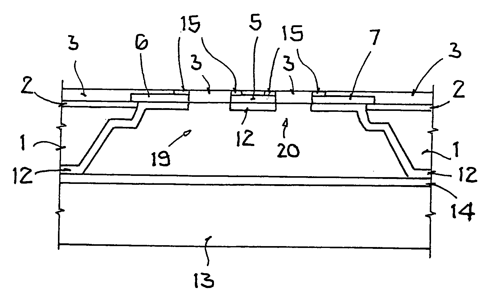
[0086]FIG. 5 illustrates a cross-sectional view of the component according to the present invention. As is shown in FIG. 5, a covering metallization 16 is additionally formed over the coplanar waveguide system, whereby the respective rim regions of the covering metallization 16 are connected with the outer areas of the two grounding conductors 6 and 7. In this way, a closed system to protect the signal conductor from external interferences and dirt is constructed. In addition, the covering metallization 16 is thus arranged for a common electrical connection of all grounding conductors so that only a common mass connection is required.
PUM
| Property | Measurement | Unit |
|---|---|---|
| Thickness | aaaaa | aaaaa |
| Dielectric polarization enthalpy | aaaaa | aaaaa |
| Shape | aaaaa | aaaaa |
Abstract
Description
Claims
Application Information