

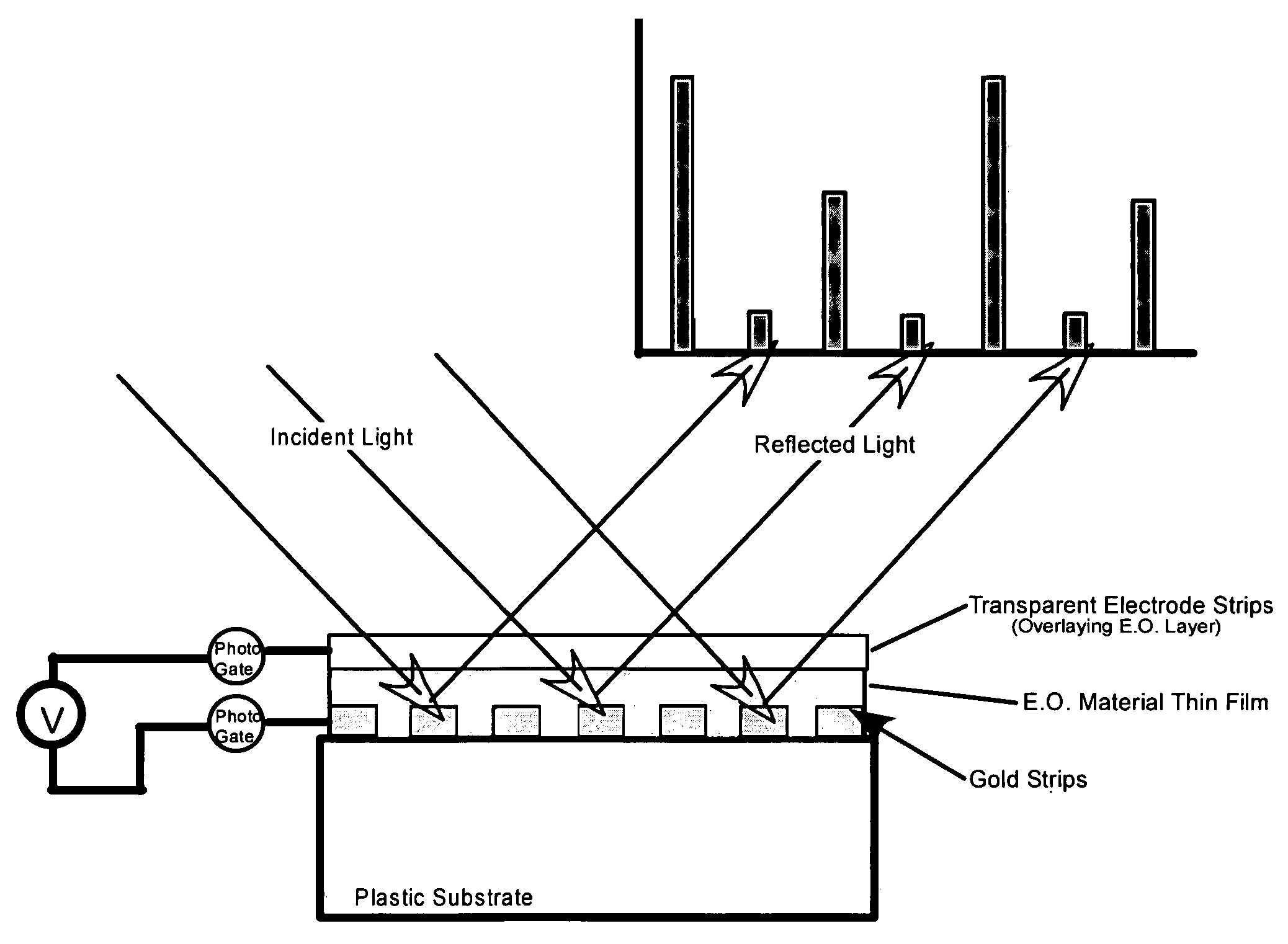
Electro-optic array interface
- Summary
- Abstract
- Description
- Claims
- Application Information
AI Technical Summary
Benefits of technology
Problems solved by technology
Method used
Image

Examples
Embodiment Construction
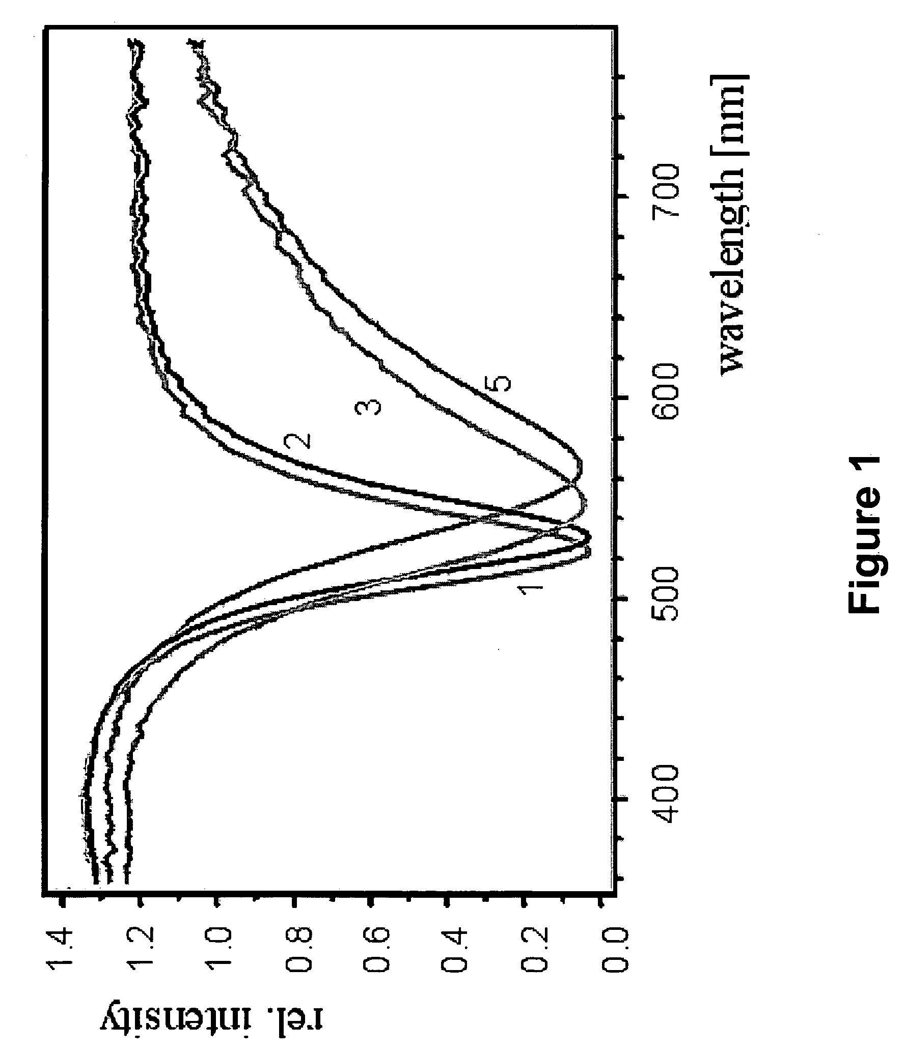
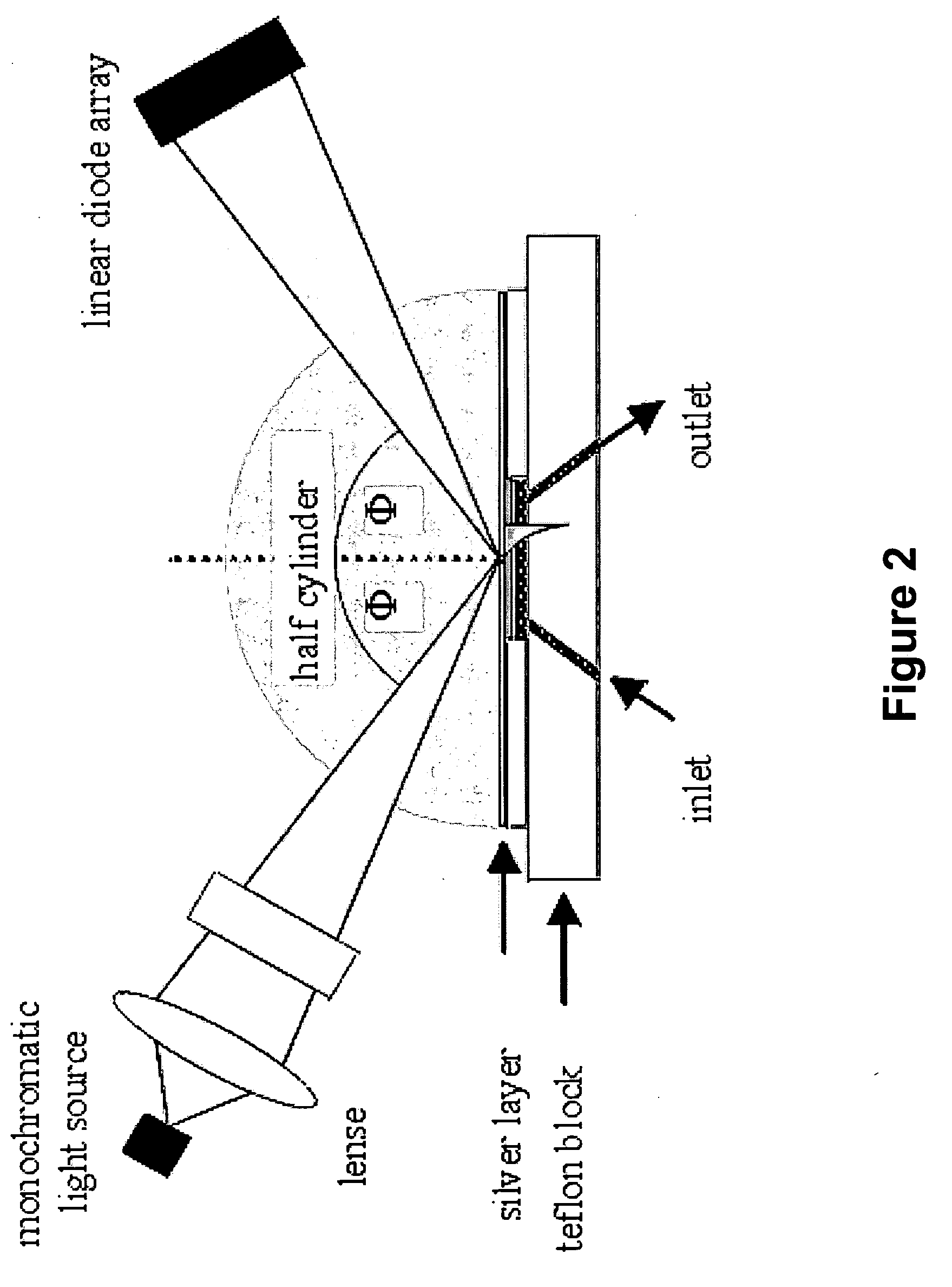
1.2.1 Surface Plasmon Resonance
[0024] At the heart of the SPROM is the high-density, dynamically reconfigurable reflector microarray. Since its function is based on grating-coupled SPR, understanding its operation and fabrication require some knowledge of the physics of SPR, which we briefly review in this section.
[0025] The theory of surface plasmon resonance is well established. When a metal surface is illuminated by TM-polarized light of the appropriate wavelength and angle of incidence, a resonance condition occurs and energy from the light is coupled into the electrons of the metal to excite what is called a surface plasmon. A surface plasmon is a propagating electron oscillation in a metal at a metal / dielectric interface. The associated electromagnetic fields constitute a guided surface mode of the conductor-dielectric interface and are evanescent in each medium with intensity decaying exponentially away from the surface. Penetration into the dielectric depends on the wavel...
PUM
 Abstract
Description
Claims
Application Information