Carbon nanotube composite material, magnetic material and production thereof
a carbon nanotube and composite material technology, applied in the field magnetic material and production thereof, can solve the problems of insufficient physical properties and practicability, low filling rate and insufficient control of carbon nanotube composite material production methods, etc., to achieve high filling ratio of magnetic metal, high magetnic properties, and uniform magnetic properties
- Summary
- Abstract
- Description
- Claims
- Application Information
AI Technical Summary
Benefits of technology
Problems solved by technology
Method used
Image
Examples
example 1
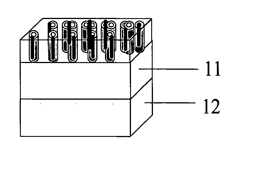
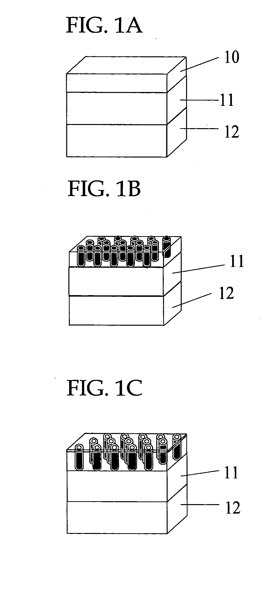
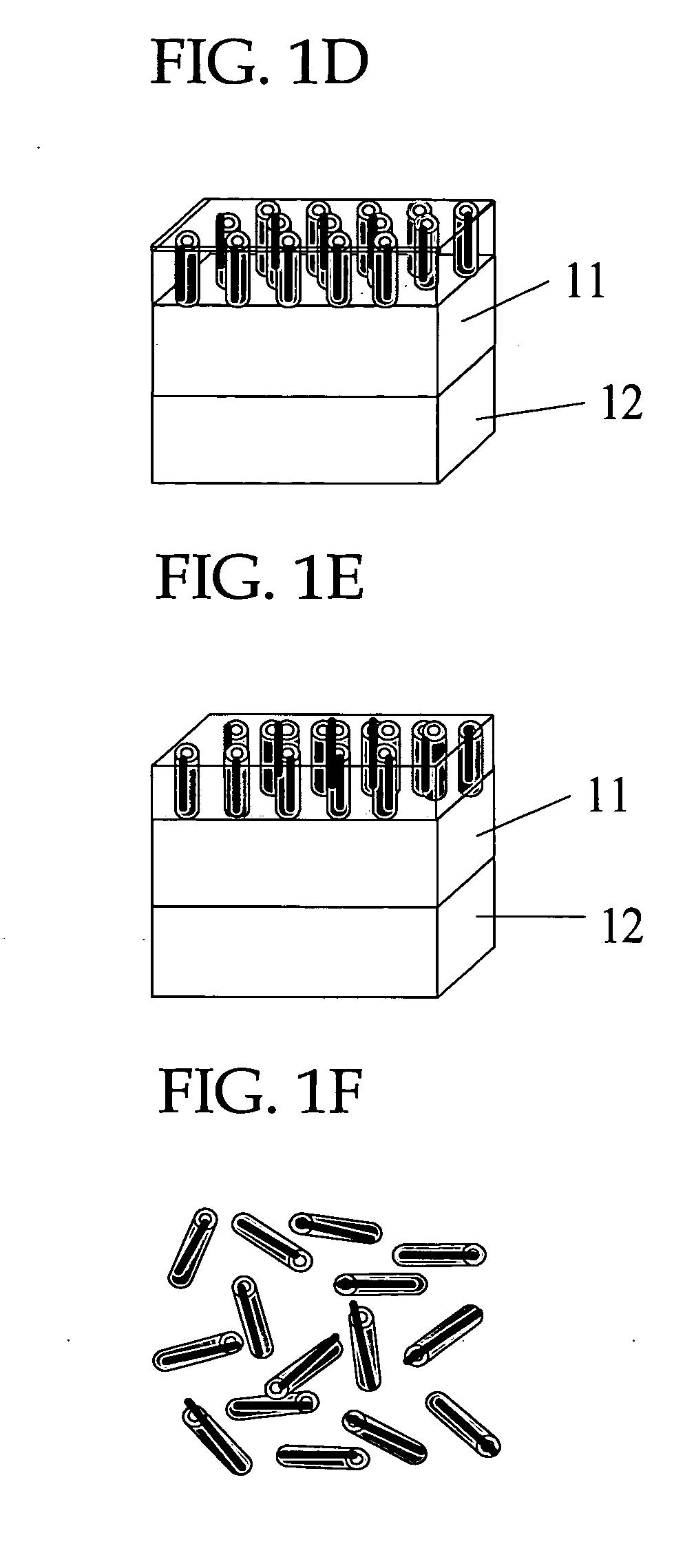
[0098] With reference to FIGS. 1A to 1F, initially, a layer 11 of Nb as the electrode layer 250 nm thick was deposited on a silicon wafer 12 in vacuo by sputtering. Then a layer 10 of aluminum (Al) as the metallic matrix layer was deposited thereon in vacuo by sputtering using an aluminum sputtering target (FIG. 1A). The resulting metallic matrix layer was anodized in a 20% by weight sulfuric acid solution at 20° C. at a voltage of 10 V to thereby form the nanohole structure having a multiplicity of nanoholes (alumina nanoholes, alumina pores) as through-holes extending in a direction substantially perpendicular to the plane of the metallic matrix layer (FIG. 1B). This process is the nanohole structure forming process.
[0099] The metallic matrix layer has a thickness (depth or length of the nanoholes) of 300 nm, and the nanoholes each have an opening with a diameter of 15 nm.
[0100] Next, carbon was allowed to grow on the outer surface of the nanohole structure (alumina nanohole) an...
example 2
[0109] A series of carbon nanotube composite materials (magnetic materials) were produced by the procedure of Example 1, except that the thickness of the metallic matrix layer was changed to 1000 nm, 500 nm, 300 nm and 50 nm, respectively, and that the plasma treatment was not carried out (FIGS. 2A to 2E). Specifically, a layer 11 of Nb as the electrode layer 250 nm thick was deposited on a silicon wafer 12 in vacuo by sputtering. Then a layer 10 of aluminum (Al) as the metallic matrix layer was deposited thereon in vacuo by sputtering using an aluminum sputtering target (FIG. 2A). The resulting metallic matrix layer was anodized in a 20% by weight sulfuric acid solution at 20° C. at a voltage of 10 V to thereby form the nanohole structure having a multiplicity of nanoholes (alumina nanoholes, alumina pores) as through-holes extending in a direction substantially perpendicular to the plane of the metallic matrix layer (FIG. 2B). Next, carbon was allowed to grow on the outer surface ...
example 3
[0111] Carbon nanotube composite materials (magnetic materials) were produced by the procedure of Example 1, except that the plasma treatment was carried out before the continuous layer coating process (FIGS. 3A to 3E). Specifically, a layer 11 of Nb as the electrode layer 250 nm thick was deposited on a silicon wafer 12 in vacuo by sputtering. Then a layer 10 of aluminum (Al) as the metallic matrix layer was deposited thereon in vacuo by sputtering using an aluminum sputtering target (FIG. 3A). The resulting metallic matrix layer was anodized in a 20% by weight sulfuric acid solution at 20° C. at a voltage of 10 V to thereby form the nanohole structure having a multiplicity of nanoholes (alumina nanoholes, alumina pores) as through-holes extending in a direction substantially perpendicular to the plane of the metallic matrix layer (FIG. 3B). Next, carbon was allowed to grow on the outer surface of the nanohole structure (alumina nanohole) and the inner surfaces of the nanoholes by ...
PUM
| Property | Measurement | Unit |
|---|---|---|
| Length | aaaaa | aaaaa |
| Depth | aaaaa | aaaaa |
| Size | aaaaa | aaaaa |
Abstract
Description
Claims
Application Information


