Data processor

a data processor and data technology, applied in the field of data processors, can solve the problems of increasing the invalidation of data after being read, the penalty of processing cache misses, and the increase of data invalidation after being read, so as to improve the data throughput of the system, reduce the rate of access conflicts between circuit modules to the external memory, and enhance the bus throughput of the external memory.

Inactive Publication Date: 2005-12-01
RENESAS ELECTRONICS CORP
View PDF14 Cites 27 Cited by
  • Summary
  • Abstract
  • Description
  • Claims
  • Application Information

AI Technical Summary

Benefits of technology

[0023] If the memory control unit should reply the data according to the order of the access requests, that is, if it does not reorder, it will acquire the data in response to the access request that hits on the bank caches earlier than the data in response to the access request that misses on the bank caches; however, it needs to wait until the latter response in order to reply the former response to the access request originator, which in consequence deteriorates the data throughput of the system. Thus, with regard to the order of the read access commands from the circuit module, the memory control unit is capable of outputting the read data from the bank cache that has the association hit on prior to the read data from the external memory relating to the association miss of the bank cache, as the data to the read access request originator. Therefore, it does not need to wait excessively for receiving the reply to the access request.
[0024] [4] According to another aspect of the invention, the data processor includes: a memory control unit being capable of controlling synchronously with a clock an external memory having plural banks, a bus connected to the memory control unit, and a circuit module capable of commanding memory accesses and provided in correspondence with the bus. When the circuit module requests a burst read with a smaller access data size than a number of bits of the bus, the memory control unit is capable of issuing read requests continuously to the external memory with a fewer frequency than a burst length of the requested burst read. In other words, in response to an access request from the circuit module that designates a burst length with a smaller access data size than a number of bits of the bus, the memory control unit validates all the data received by one read request to the external memory, and issues read requests plural times continuously. That is, the memory control unit merges the read requests issued to the external memory according to the access requests from the circuit module. For example, when the number of bits of the bus is equal to the data bit number that can be read from the external memory in one clock cycle, and the access data size of the burst read request from the circuit module is 1 / n of the number of bits of the bus, the memory control unit merges the read requests from n-circuits to the external memory into the read request of one time. Thereby, the frequency of the read requests that the memory control unit issues to the external memory is reduced to 1 / n. The memory control unit validates all the bits of the read data from the external memory every times, and replies the data to the circuit modules according to the requested access data size. Thereby, the bus throughput of the external memory is enhanced, the rate of access conflicts between the circuit modules to the external memory is reduced, and in consequence the data throughput of the system is enhanced.

Problems solved by technology

However, when an access entity makes a memory access request with a word or long word access data size, most of the data read out from the DDR memory in one clock cycle do not satisfy the request, and they are invalidated.
For example, when the access data size of a burst access request from a CPU or the like is smaller than the access data size in one clock cycle, and when the memory access in one clock cycle is repeated each time by a designated burst access frequency, there increase data invalidated after being read.
In such a CPU cache memory, the processing of cache miss penalty in performing entry by a cache miss or replacement of a cache line is considerably heavy; therefore, it becomes important to cover the programs and data being used repeatedly in the cache objects.

Method used


Image

  • Data processor
  • Data processor
  • Data processor

Examples


Embodiment Construction

[Image Processor]

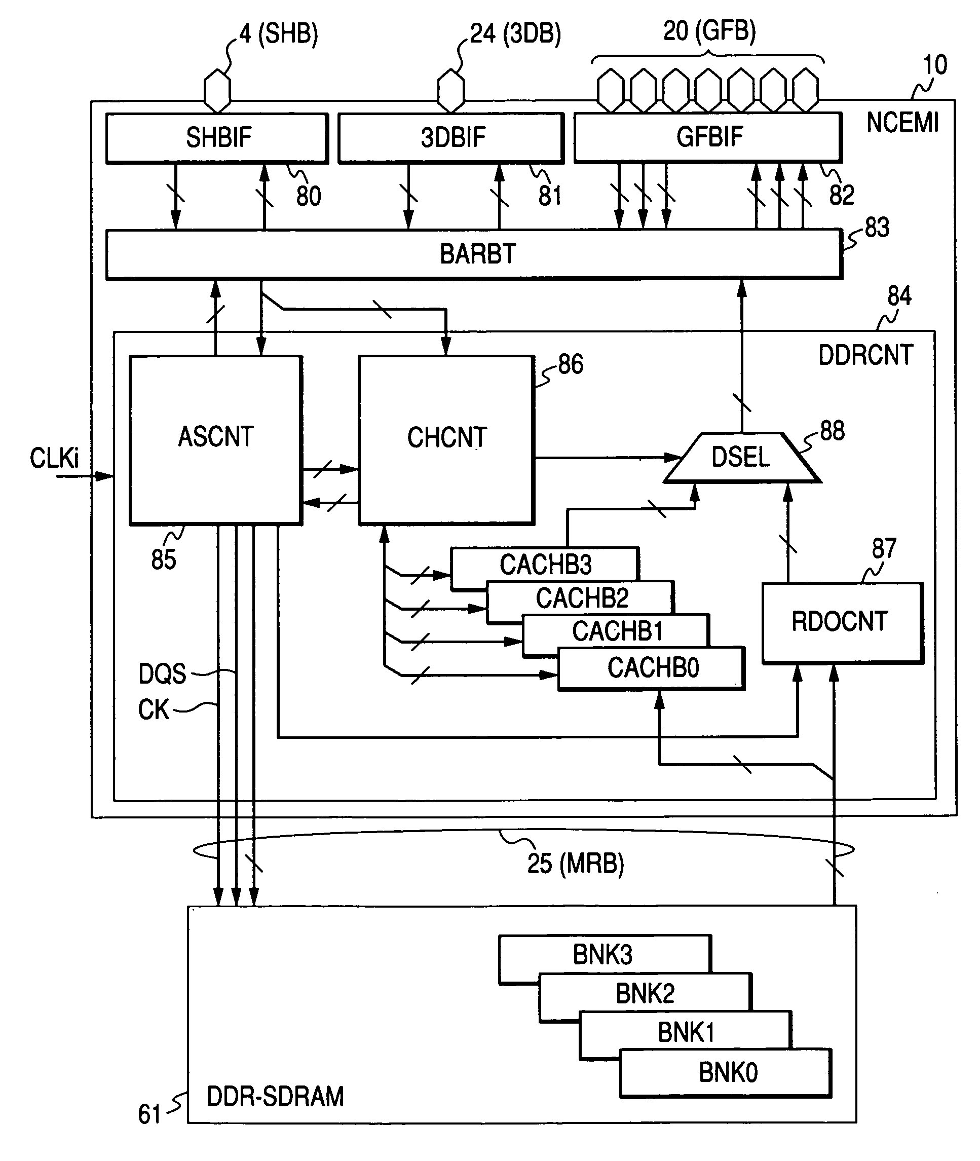
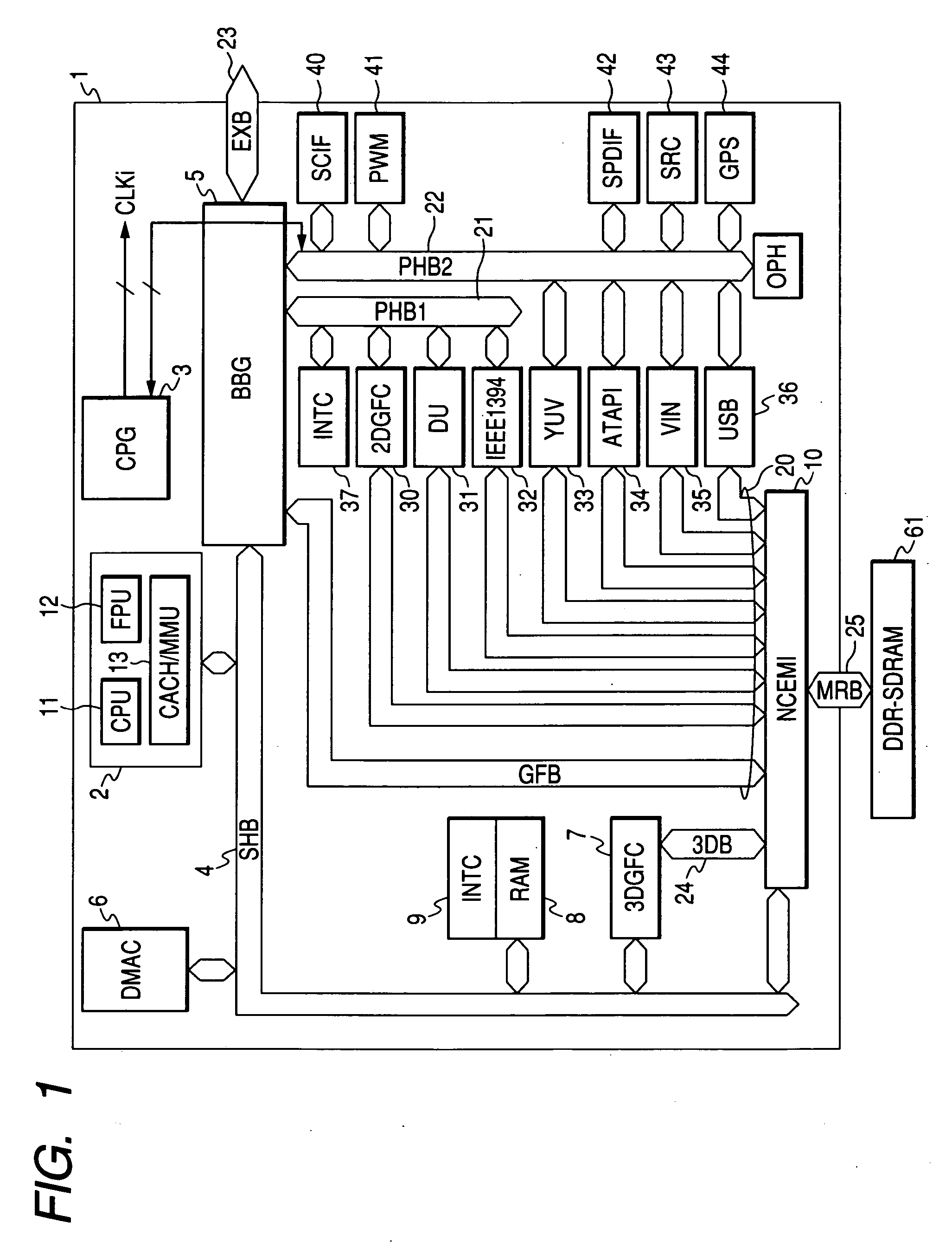
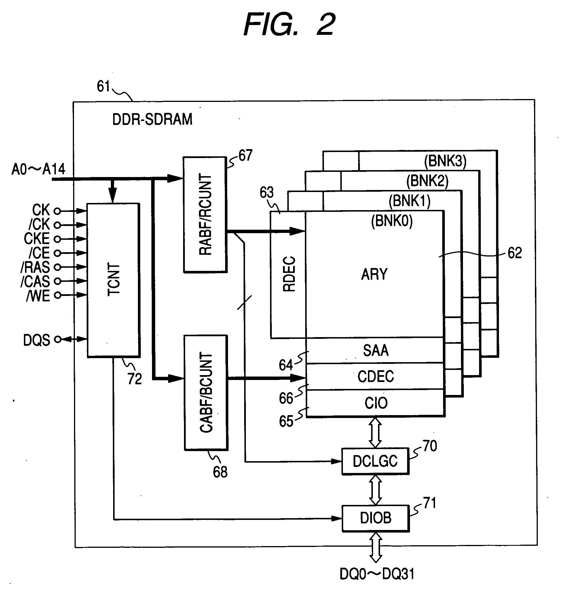
[0048]FIG. 1 illustrates an image processor as an example according to this invention. An image processor 1 illustrated in the drawing is formed on one semiconductor substrate (semiconductor chip) of a single crystal silicon and the like by means of the manufacturing technique of complimentary MOS (CMOS) integrated circuits, which is not specifically stipulated. The image processor 1 includes image processing and sound processing functions necessary for the car navigation and a DDR-SRAM (Double Data Rate Synchronous Dynamic Random Access Memory) interface and so forth.

[0049] The image processor 1 includes a processor core 2 and a clock pulse generator (CPG) 3. The processor core 2 is connected to a super highway bus (SHB) 4. The super highway bus (SHB) 4 is connected with a bus bridge circuit (BBRG) 5, a direct memory access controller (DMAC) 6, a 3D engine (3DGFC) 7 that performs the three-dimensional image processing such as three-dimensional graphic drawings, a...


PUM


Abstract

The data processor enhances the bus throughput or data throughput of an external memory, when there are frequent continuous reads with a smaller data size than the data bus width of the external memory. The data processor includes a memory control unit being capable of controlling in response to a clock an external memory having plural banks that are individually independently controllable, plural buses connected to the memory control unit, and circuit modules capable of commanding memory accesses, which are provided in correspondence with each of the buses. The memory control unit contains bank caches each corresponding to the banks of the external memory. Thereby, the data processor enhances the bus throughput or data throughput of the external memory, since the data processor stores the data read out from the external memory temporarily in the bank caches and to use the stored data without invalidating them, when performing a continuous data read with a smaller data size than the data bus width of the external memory.

Description

CROSS REFERENCE TO RELATED APPLICATION [0001] The present application claims priority from Japanese patent application No. 2004-159510 filed on 28 May, 2004, the content of which is hereby incorporated by reference into this application. BACKGROUND OF THE INVENTION [0002] The present invention relates to a data processor having a memory controller capable of controlling an external memory synchronously with a clock, specifically to a technique effective in use for a microcontroller provided with an interface controller for a DDR-SDRAM (double data rate SDRAM) memory. [0003] The synchronous memory that behaves synchronously with a clock, represented by an SDRAM (Synchronous Dynamic Random Access Memory), is widely used for a frame buffer for graphics and a main memory in a CPU (Central Processing Unit) and so forth. For example, the SDRAM has plural memory banks, and each memory bank has an address decoder, memory array, sense amplifier array, and so forth, and each is made independe...

Claims


Application Information

Patent Timeline
Patent Type & Authority Applications(United States)
IPC IPC(8): G06F12/08G06F12/00G06F12/04G06F13/16
CPCG06F13/1678G06F12/0875
Inventor KATSUKI, FUMIENARUSE, TAKANOBUFUJII, CHIAKI
Owner RENESAS ELECTRONICS CORP
Why Eureka
Try Eureka