

III-V group nitride system semiconductor self-standing substrate, method of making the same and III-V group nitride system semiconductor wafer
a nitride system and semiconductor technology, applied in the direction of crystal growth process, polycrystalline material growth, chemically reactive gas growth, etc., can solve the problem of difficult to grow a bulk crystal of nitride system semiconductor, number of dislocations (defects) must be generated in grown crystals, and difficulty in flattening the surface morphology of the substrate. achieve good flatness, uniformity and reproducibility
- Summary
- Abstract
- Description
- Claims
- Application Information
AI Technical Summary
Benefits of technology
Problems solved by technology
Method used
Image

Examples
example 1
(Manufacture of GaN Self-Standing Substrate by VAS)
[0110] Referring to FIGS. 4A to 4G, the manufacture of a GaN self-standing substrate by the VAS method will be explained below.
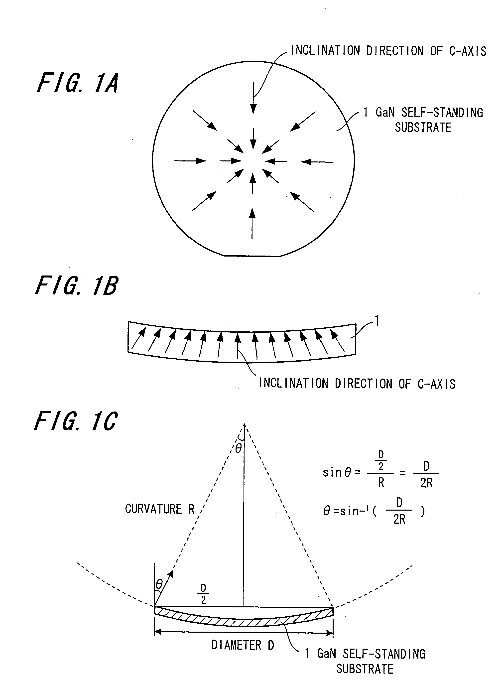
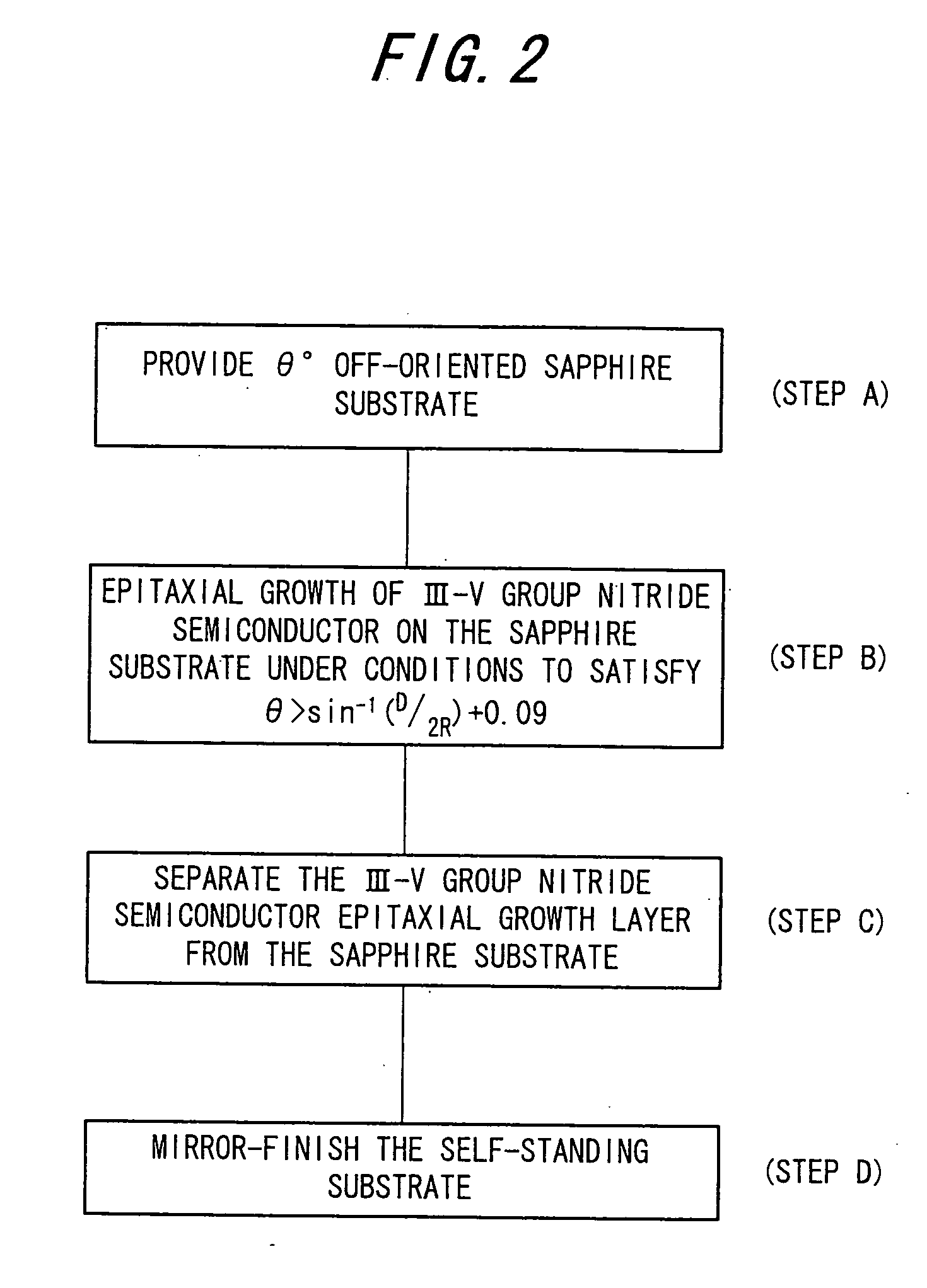
[0111] At first, a commercially-available single-crystal sapphire C-face substrate 21 with a diameter of 2 inches is provided that is off-oriented 0.25 degrees in the m-axis direction (FIG. 4A).
[0112] Then, a 300 nm undoped GaN layer 22 is grown on the sapphire substrate 21 by MOVPE using TMG, NH3 as raw materials (FIG. 4B). Then, a 20 nm Ti film 23 is deposited on the GaN epi-substrate (FIG. 4C), entered into an electric oven, and heated at 1050° C. for 20 min in H2 flow with 20% NH3 mixed therein. Thereby, the Ti film 23 is processed into a mesh-like slotted TiN layer 25 and simultaneously the GaN layer 22 is processed into a void-formed GaN layer 24 (FIG. 4D).
[0113] This is entered in an HVPE furnace, and then a 700 μm GaN layer 26 is deposited (FIG. 4E). NH3 and GaCl are used raw materials and mixed...
example 2
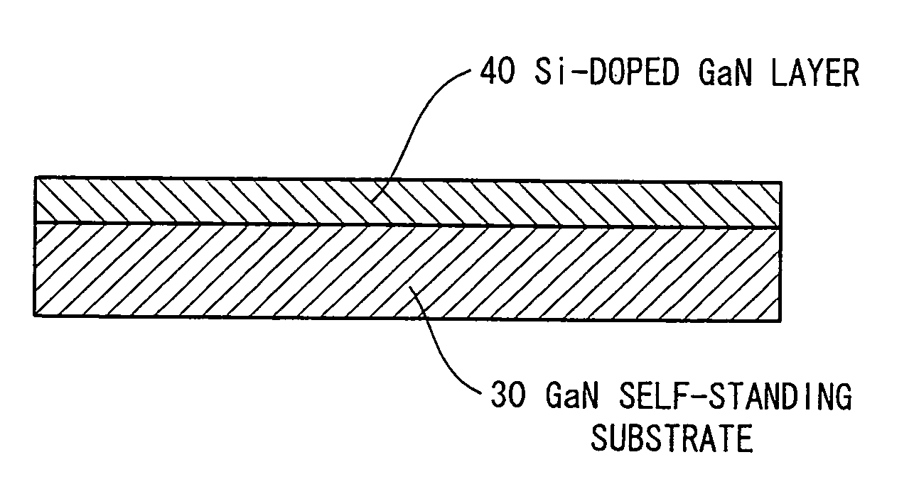
(Formation of GaN Layer on GaN Self-Standing Substrate)
[0120] As shown in FIG. 7, a 2 μm Si-doped GaN layer 40 is grown on the GaN self-standing substrate 30 manufactured in Example 1 by MOVPE. The growth pressure of GaN layer 40 is atmospheric pressure and the growth temperature of self-standing substrate 30 is 1100° C. TMG is used as III group raw material, NH3 as V group material, and monosilane as dopant. The carrier gas is mixed gas of hydrogen and nitrogen. The growth rate of crystal is 4 μm / h, and target carrier concentration of epi-layer is 2×1018 cm3.
[0121] The surface of GaN layer 40 obtained is observed by Nomarski microscope. Although in most areas is observed a linear morphology that is assumed to be formed due to step bunching, only in a limited area is observed a region A that hexagonal uneven patterns of about 5 to 20 μm are collected. FIG. 8 shows the position of region A.
[0122] As the result of measuring the inclination of crystal C-axis inside and outside the ...
example 3
(Manufacture of GaN Self-Standing Substrate by VAS)
[0123] In analogy with Example 1, a GaN self-standing substrate is manufactured by the VAS method as shown in FIGS. 4A to 4G.
[0124] At first, a commercially-available single-crystal sapphire C-face substrate 21 with a diameter of 2 inches is provided that is off-oriented 0.30 degrees in the m-axis direction (FIG. 4A).
[0125] Then, a 300 nm undoped GaN layer 22 is grown on the sapphire substrate 21 by MOVPE using TMG, NH3 as raw materials (FIG. 4B). Then, a 20 nm Ti film 23 is deposited on the GaN epi-substrate (FIG. 4C), entered into an electric oven, and heated at 1050° C. for 20 min in H2 flow with 20% NH3 mixed therein. Thereby, the Ti film 23 is processed into a mesh-like slotted TiN layer 25 and simultaneously the GaN layer 22 is processed into a void-formed GaN layer 24 (FIG. 4D).
[0126] This is entered in an HVPE furnace, and then a 700 μm GaN layer 26 is deposited (FIG. 4E). NH3 and GaCl are used raw materials and N2 is u...
PUM
 Abstract
Description
Claims
Application Information