III-V group nitride system semiconductor self-standing substrate, method of making the same and III-V group nitride system semiconductor wafer

Inactive Publication Date: 2005-12-15
HITACHI CABLE
View PDF1 Cites 20 Cited by
  • Summary
  • Abstract
  • Description
  • Claims
  • Application Information

AI Technical Summary

Benefits of technology

[0036] It is advantageous that the III-V group nitride system semiconductor self-standing substrate of the invention can offer an epitaxial growth layer with high flatness, uniformity and reproducibility when epitaxially growing a nitride system semiconductor layer on the self-standing substrate.
[0037] Further, it is advantageous that the method of making a III-V group nitride system semiconductor self-standing substrate of the invention can offer a III-V group nitride system semiconductor substrate with a suitable off-orientation with a good reprodu

Problems solved by technology

On the other hand, it is difficult to grow a bulk crystal of nitride system semiconductor, and a GaN self-standing substrate did not exist before the epitaxial growth of nitride is researched.
However, in the hetero-epitaxial growth on hetero-substrate, a number of dislocations (defects) must be generated in grown crystal due to a lattice mismatch between the underlying substrate and the grown crystal.
However, even when such a GaN self-standing substrate is used to grow a GaN system epitaxial layer thereon, it is difficult to flatten its surface morphology in the epitaxial growth wh

Method used


Image

  • III-V group nitride system semiconductor self-standing substrate, method of making the same and III-V group nitride system semiconductor wafer
  • III-V group nitride system semiconductor self-standing substrate, method of making the same and III-V group nitride system semiconductor wafer
  • III-V group nitride system semiconductor self-standing substrate, method of making the same and III-V group nitride system semiconductor wafer

Examples


example 1

[0068] Manufacture of GaN Self-Standing Substrate

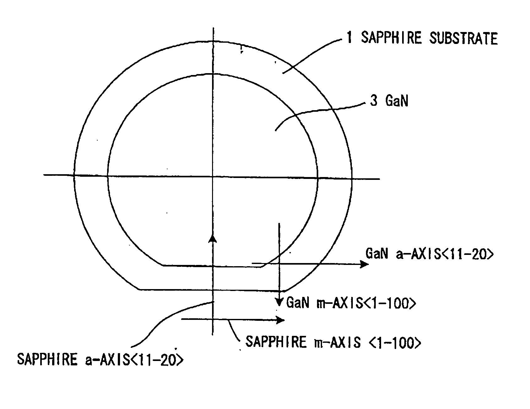
[0069] A GaN self-standing substrate is manufactured by a process as shown in FIG. 4. At first, single-crystal sapphire C-face substrates 21 with a diameter of 2 inches are provided that are each off-oriented 0.1, 0.5, 1, 3, 8, 15, 20 and 21 degrees in the m-axis direction (FIG. 4A).

[0070] Then, a 300 nm undoped GaN layer 22 is grown on the sapphire substrate 21 by MOVPE using TMG, NH3 as raw materials (FIG. 4B). Then, 20 nm Ti film 23 is deposited on the GaN epi-substrate (FIG. 4C), entered into an electric oven, and heated at 1050° C. for 20 min in H2 flow with 20% NH3 mixed therein. Thereby, Ti film 23 is processed into a mesh-like slotted TiN layer 25 and simultaneously the GaN layer 22 is processed into a void-formed GaN layer 24 (FIG. 4D).

[0071] This is entered in an HVPE furnace, and then a 500 μm GaN layer 26 is deposited (FIG. 4E). NH3 and GaCl are used raw materials and N2 is used as carrier gas. The growth conditions are...

example 2

[0075] Formation of GaN Layer on the GaN Self-Standing Substrate

[0076] The GaN self-standing substrates with different off-angles manufactured in Example 1 are mirror-finished by polishing on both surfaces. Then, as shown in FIG. 6, a 4 μm undoped layer 15 is grown on the GaN self-standing substrate 11 by MOVPE using TMG (trimethylgallium) and NH3 as raw materials. In the MOVPE growth, the growth pressure is atmospheric and the substrate temperature is 1050° C. The carrier gas is mixed gas of hydrogen and nitrogen. The crystal growth rate is about 4 μm / h.

[0077] The surface of epitaxial undoped GaN layer 15 thus obtained appears to be a mirror surface to the naked eye. However, when observing the surface by the Nomarski microscope, a number of microscopic hexagonal hillocks with a diameter of about 50 to 200 μm are generated on the surface of an epitaxial layer grown on substrates with an off-angle of less than 0.09 degrees. In contrast, on the surface of an epitaxial layer grown o...


PUM


Abstract

A III-V group nitride system semiconductor self-standing substrate is made of III-V group nitride system semiconductor single crystal with a hexagonal crystal system crystalline structure. The substrate is provided with a surface that is off-oriented 0.09 degrees or more and 24 degrees or less in the a-axis or m-axis direction from C-face of the substrate.

Description

[0001] The present application is based on Japanese patent application No. 2004-162189, the entire contents of which are incorporated herein by reference. BACKGROUND OF THE INVENTION [0002] 1. Field of the Invention [0003] The present invention relates to a III-V group nitride system semiconductor self-standing substrate, a method of making the same, a III-V group nitride system semiconductor wafer. [0004] 2. Description of the Related Art [0005] Nitride system semiconductor materials such as gallium nitride (GaN), indium gallium nitride (InGaN) and gallium aluminum nitride (GaAlN) have a sufficiently wide bandgap and are of direct transition type in inter-band transition. Therefore, they are a great deal researched to be used for short-wavelength light emitting devices. Further, they have a high saturation drift velocity of electron and can use two-dimensional carrier gases in hetero junction. Therefore, they are also expected to be used for electronic devices. [0006] With silicon ...

Claims


Application Information

Patent Timeline
IPC IPC(8): C30B25/18C30B29/60C30B29/38C30B29/40C30B25/02H01L31/072H01L21/28
CPCC30B25/02C30B25/18C30B29/40C30B29/64Y10S438/977
Inventor SHIBATA, MASATOMO
Owner HITACHI CABLE
Why Eureka
Try Eureka