Apparatus and methods for overlay, alignment mark, and critical dimension metrologies based on optical interferometry

a technology of optical interferometry and overlay, applied in the field of multi-layer structure manufacturing, can solve the problems of difficult reduction of tis, inaccurate reflection of circuit features themselves, accuracy issues, etc., and achieve the effect of reducing the sensitivity of overlay measurement errors

Inactive Publication Date: 2005-12-15
ZETETIC INST
View PDF64 Cites 38 Cited by
  • Summary
  • Abstract
  • Description
  • Claims
  • Application Information

AI Technical Summary

Benefits of technology

[0073] a reduced sensitivity of the measurement of overlay errors, a...

Problems solved by technology

Although this has worked well, there are several issues as the industry moves toward implementing deep nanometer process levels with for example image overlay tools, location of alignment marks used in a stage metrology system of lithography tool or inspection tool, and measurement of properties such as CDs.
With respect to overlay metrology, one of these issues has to do with the traditionally used BiB structures which tend to have large geometries and typically consist of bars microns in size that do not correspond to circuit feature sizes.
As increasingly smaller features are being produced, it has become apparent that the behavior of these traditional BiB targets does not accurately reflect that of the circuit features themselves.
Now, smaller geometries are resulting in accuracy issues that must be addressed in imaging overlay tools, in particular the tool-induced shift (TIS).
Imaging overlay makes it difficult to reduce TIS because it is critically dependent upon residual aberrations in the imaging overlay optics with the most critical one being the microscope objective.
Strehl ratios as high as 0.9 often do not provide the TIS performance required for advanced design rules.
Thus, the technology faces not only optical problems but the fact that traditional overlay marks do not represent the actual behavior of circuit features that are orders of magnitude smaller.
Typically, the allowable overlay error is ⅓ of the CD in the IC device.
Alignment issue is more severe in a back-end process partly due to the influence of CMP, which contributes to the asymmetric or total destruction of the alignment marks.
However, reduced physical size of alignment marks and of overlay patterns used in overlay metrology reduces the magnitude of the diffracted signals detected in determination of alignment marks and overlay errors, respectively.
The problems that arise in an optical measurement of a CD can also include those introduced by TIS and WIS.
Relative vibration would blur the image and degrade the performance.
This is a difficult requirement to meet for overlay metrology systems that are integrated into a process tool.
The tool causes potentially large accelerati...

Method used


Image

  • Apparatus and methods for overlay, alignment mark, and critical dimension metrologies based on optical interferometry
  • Apparatus and methods for overlay, alignment mark, and critical dimension metrologies based on optical interferometry
  • Apparatus and methods for overlay, alignment mark, and critical dimension metrologies based on optical interferometry

Examples


first embodiment

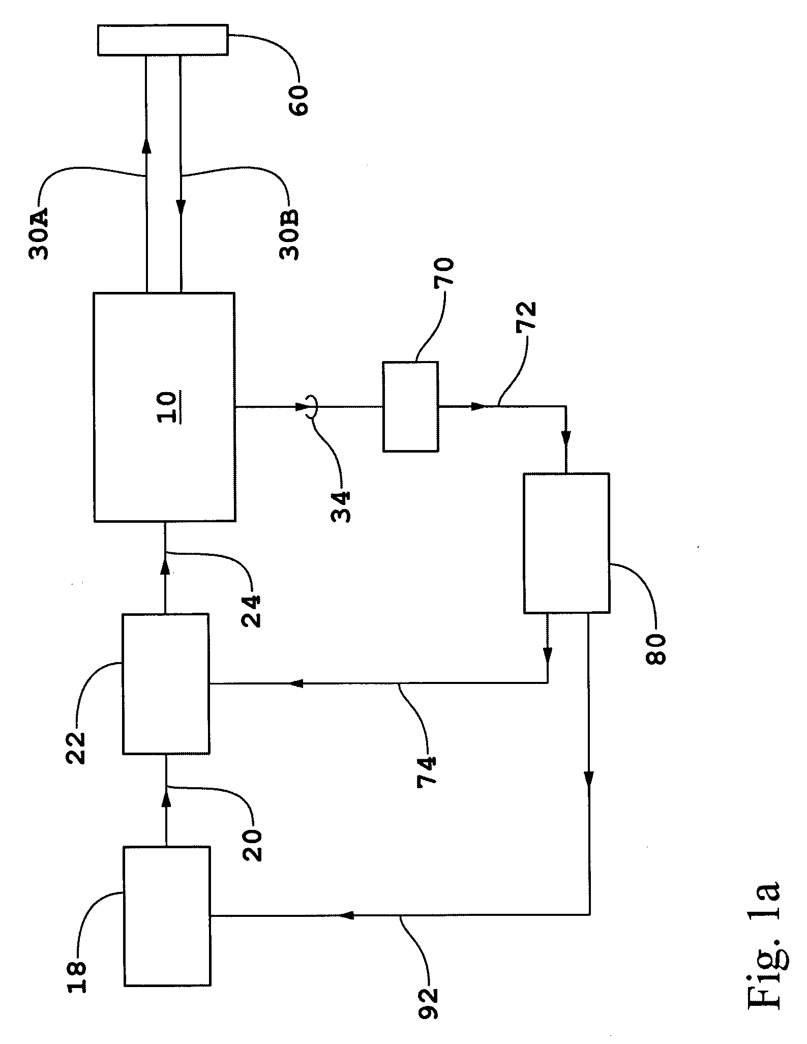
[0226] Two different modes are described for the acquisition of the electrical interference signals 72 of the The first mode to be described is a step and stare mode wherein substrate 60 is stepped between fixed locations corresponding to locations where image information is desired. The second mode is a scanning mode. In the step and stare mode for generating a one-dimensional, a two-dimensional or a three-dimensional profile of substrate 60, substrate 60 mounted in wafer chuck 84 is translated by stage 90 (see FIG. 1c). The position of stage 90 is controlled by transducer 82 according to servo control signal 78 from electronic processor and controller 80. The horizontal position of stage 90 is measured by metrology system 88 and position information acquired by metrology system 88 is transmitted to electronic processor and controller 80 to generate an error signal for use in the position control of stage 90. Metrology system 88 may comprise for example linear displacement and ang...

third embodiment

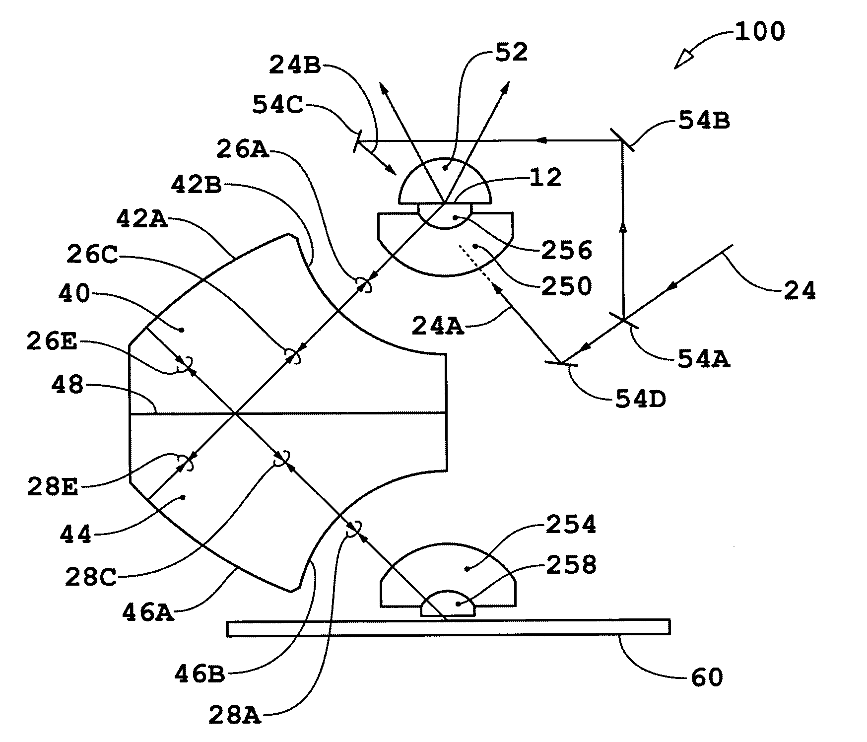
[0257] An advantage of the third embodiment is that information can be obtained about the measurement object using one or more of the two complimentary oblique measurement beams and non-oblique measurement with a single interferometric metrology system without rotation of either the measurement object or the interferometric metrology system and without changes in the relative location of the single interferometric metrology system with respect to the measurement object in the z direction to make for example overlay metrology measurements. In particular, information about two different surfaces of a measurement object can be obtained simultaneously.

[0258] In the third embodiment of the present invention, the information obtained about the location of feature on a measurement object in a plane parallel to the surface of the measurement object is obtained operating in a scanning mode as with each of various embodiments of the present invention. The statistical and systematic errors in ...


PUM


Abstract

Methods and apparatus based on optical homodyne displacement interferometry, optical coherent-domain reflectometry (OCDR), and optical interferometric imaging are disclosed for overlay, alignment mark, and critical dimension (CD) metrologies that are applicable to microlithography applications and integrated circuit (IC) and mask fabrication and to the detection and location of defects in/on unpatterned and patterned wafers and masks. The metrologies may also be used in advanced process control (APC), in determination of wafer induced shifts (WIS), and in the determination of optical proximity corrections (OPC).

Description

[0001] This application claims the benefit of U.S. Provisional Application No. 60 / 573,196, filed May 21, 2004, incorporated herein by reference. RELATED APPLICATIONS [0002] The following patents and patent applications are related to the present application: U.S. Pat. No. 6,445,453, entitled “Canning Interferometric Near-Field Confocal Microscopy” (ZI-14); and U.S. patent application Ser. No. 10 / 778,371, filed Feb. 13, 2004, entitled “Transverse Differential Interferometric Confocal Microscopy,” (ZI-40); Ser. No. 10 / 782,057, filed Feb. 19, 2004, entitled “Longitudinal Differential Interferometric Confocal Microscopy for Surface Profiling,” (ZI-41); Ser. No. 10 / 782,058, filed Feb. 19, 2004, entitled “Method and Apparatus for Dark Field Interferometric Confocal Microscopy,” (ZI-42); Ser. No. 10 / 771,785, filed Feb. 4, 2004, entitled “Compensation For Effects Of Mismatch In Indicies Of Refraction At A Substrate-Medium Interface In Non-Confocal, Confocal, And Interferometric Confocal Mic...

Claims


Application Information

Patent Timeline
IPC IPC(8): G01B9/02G01B11/24G03F9/00
CPCG01B11/2441G03F9/7034G03F9/7049G01B9/02079G01B9/02072G01B9/02014G01B9/02042G01B2290/70G01B9/02002
Inventor HILL, HENRY ALLEN
Owner ZETETIC INST
Why Eureka
Try Eureka