Organic semicounductor device, process for producing the same, and organic semiconductor apparatus
a semi-counductor and organic semiconductor technology, applied in the direction of semiconductor/solid-state device details, solid-state devices, transistors, etc., can solve the problems of insufficient orientation of crystals of organic semiconductors, difficult to produce a substrate with a large area, and less versatility, and achieve the effect of low cos
- Summary
- Abstract
- Description
- Claims
- Application Information
AI Technical Summary
Benefits of technology
Problems solved by technology
Method used
Image

Examples
synthetic example 1
[0063] An example of synthesis of a copolymer of methyl methacrylate and divinylbenzene used in the organic semiconductor device of the present invention is shown in the following reaction formula (1).
[0064] A mixed solution of methyl methacrylate, divinylbenzene and a polymerization initiator was dropped in a reflux of toluene at a reflux temperature of toluene (110° C. to 120° C.). The mixture was then cooled to 80° C., and maintained at that temperature for three hours. After allowing to be cooled, the mixture was reprecipitated in methanol. After decanting the supernatant and washing the precipitate with methanol, the precipitate was filtered. The filtrate was dried by heating under reduced pressure to obtain the target polymer.
[0065] From the results of analyzing the 1H-NMR spectrum of the resulting polymer (using a 1H-NMR analyzer manufactured by JEOL Ltd., resonant frequency: 400 MHz, solvent: CDCl3, external reference material: TMS, measured at room temperature), the copo...
example 1
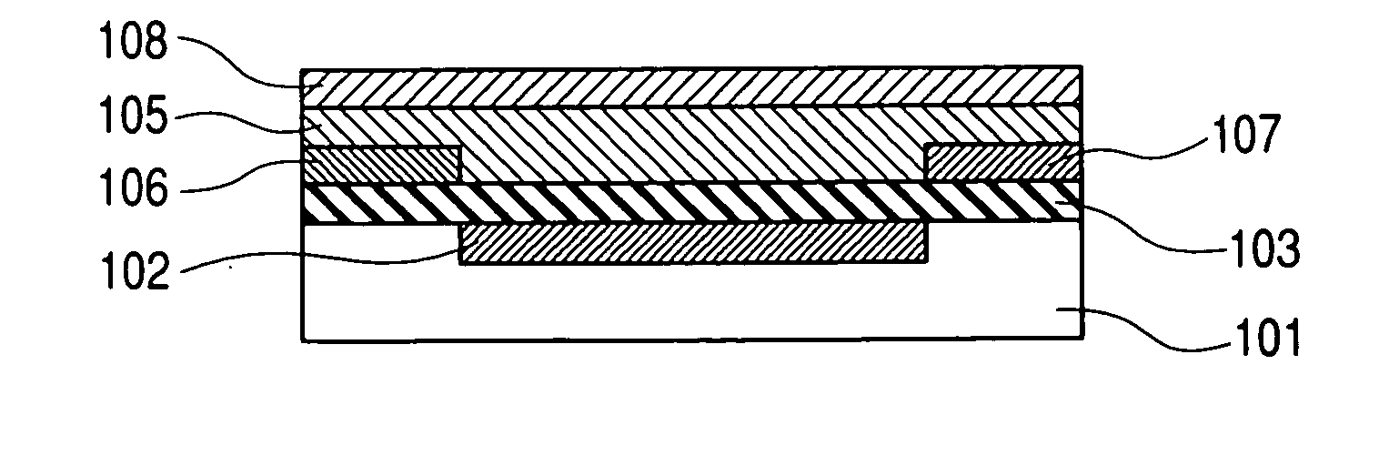
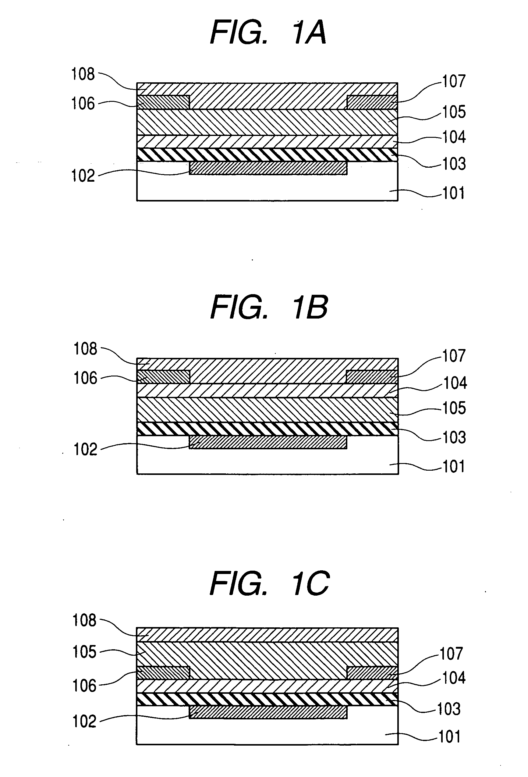
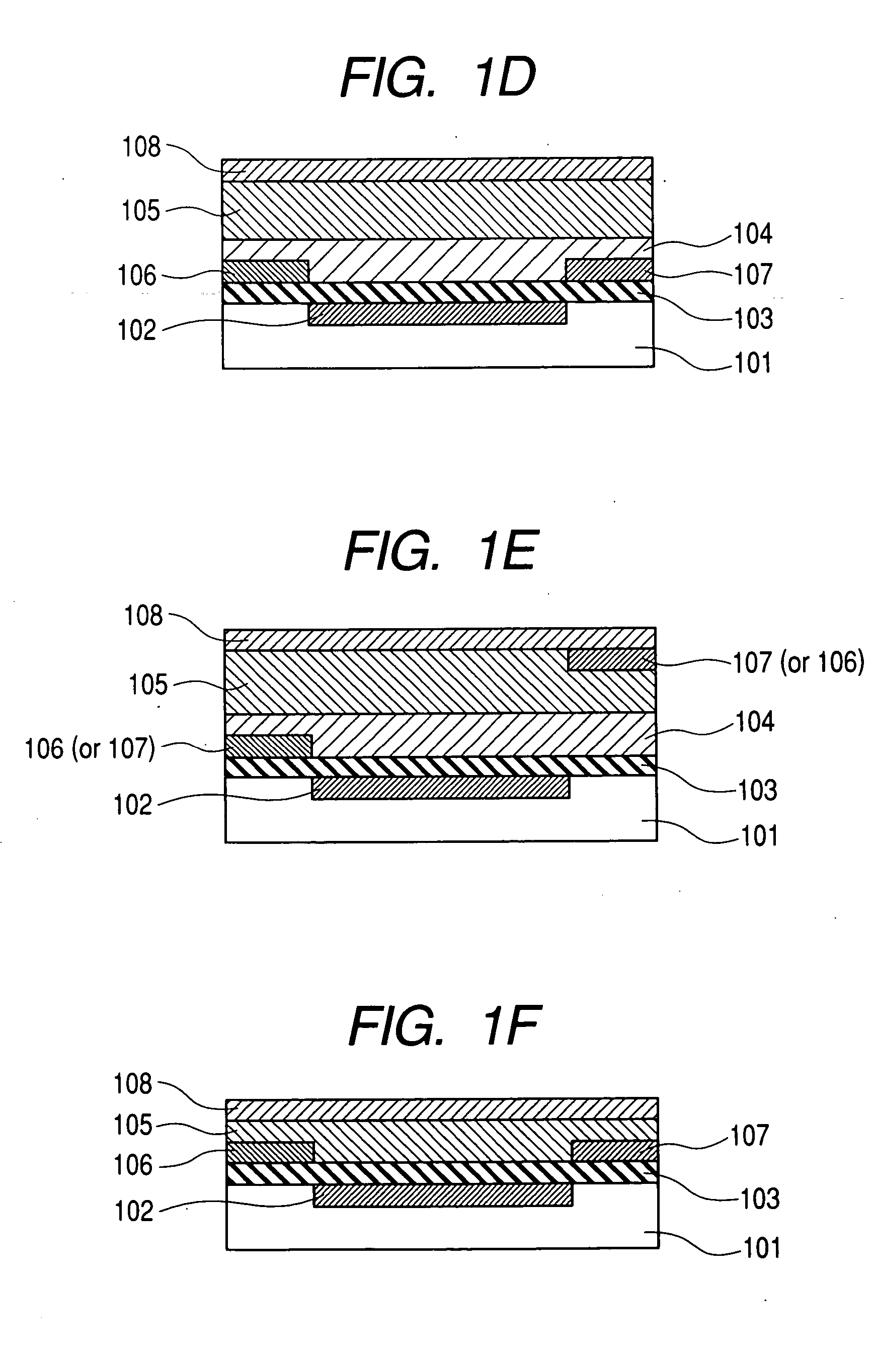
[0067] A polyimide substrate was used in this example. Upilon (trade name) manufactured by Ube Industries, Ltd. with a thickness of 125 μm was used as the substrate.
[0068] Next, copper was formed as a film by sputtering, and the film was patterned by photolithography to produce a gate electrode wire. Further, a coating-type insulating film composed of methylsilsesquioxane was formed thereon, and baked at 230° C. to form a substrate for a semiconductor.
[0069] The polyimide substrate was washed in the following manner. A step of ultrasonically washing the polyimide substrate in acetone with a purity of 99% or more for one minute and then a step of washing the substrate ultrasonically in pure water for five minutes were carried out twice, respectively. After the washing, the pure water was blowed away by an N2 gas. Then, the substrate was irradiated with ultraviolet (UV) lights at wavelengths of 184.9 nm and 253.7 nm at an intensity of 100 mW for an irradiation time of 20 seconds to ...
examples 2 to 17
[0084] Each transistor was produced in the same manner as in Example 1, while the copolymerization rate (B / A) of the polymer layer on the insulating film was changed in the range of 0.001 to 0.04. The results are shown in Table 1.
TABLE 1Comparison of copolymerization ratio of polymer layerwith transistor characteristics(Film thickness: 20 nm)CopolymerizationConditionMobilityON / OFFVthExamplerateof coating(cm2 / Vs)ratio(V)10.011Good1.122.20E+08−520.001Good0.652.90E+08−1230.002Good0.683.20E+08−1540.003Good0.765.20E+08−1650.004Good0.834.80E+08−1860.005Good0.755.10E+08−1970.006Good0.696.20E+08−1580.007Good0.898.20E+08−1290.008Good1.057.70E+08−19100.009Good1.129.25E+08−21110.01Good1.351.23E+08−22120.015Good1.21.22E+08−23130.02Good1.021.02E+08−15140.025Good0.66.50E+07−12150.03Good0.63.20E+07−12160.035Good0.31.20E+07−6170.04Good0.329.50E+06−5
PUM
| Property | Measurement | Unit |
|---|---|---|
| Thickness | aaaaa | aaaaa |
| Thickness | aaaaa | aaaaa |
| Thickness | aaaaa | aaaaa |
Abstract
Description
Claims
Application Information
 - R&D
- Intellectual Property
- Life Sciences
- Materials
- Tech Scout
- Unparalleled Data Quality
- Higher Quality Content
- 60% Fewer Hallucinations
Browse by: Latest US Patents, China's latest patents, Technical Efficacy Thesaurus, Application Domain, Technology Topic, Popular Technical Reports.
© 2025 PatSnap. All rights reserved.Legal|Privacy policy|Modern Slavery Act Transparency Statement|Sitemap|About US| Contact US: help@patsnap.com