Doped nitride film, doped oxide film and other doped films

a technology of oxide film and nitride film, which is applied in the field of films, can solve the problems of difficult to modulate stress to a large extent without comprising film quality, many low temperature precursors have been investigated, and achieve the effect of increasing the deposition ra

Inactive Publication Date: 2005-12-29
GLOBALFOUNDRIES INC
View PDF22 Cites 98 Cited by
  • Summary
  • Abstract
  • Description
  • Claims
  • Application Information

AI Technical Summary

Benefits of technology

[0005] It is therefore an object of the present invention to provide increased deposition rate compared to conventional processes, thus providing for more manufacturable films, especially silicon nitride films, silicon oxide films, silicon oxynitride films, and silicon carbide films.
[0006] Another object of the present invention is to provide the ability to produce good quality nitride films of varying stress levels, thus enhancing device performance as a “plug-in” solution, i.e., with no integration changes needed.
[0007] Another object of the present invention is to lower the temperature for deposition of a silicon nitride film, a silicon oxide film, a silicon oxynitride film or a silicon carbide film.
[0008] A further object of the present invention is to manipulate germanium addition during production of a silicon nitride film, silicon oxide film, silicon oxynitride film or silicon carbide film, to control stress in the produced film.

Problems solved by technology

However, within a given deposition regime it only has been possible to modulate the stress within a small range.
It has been very difficult to modulate the stress to a large extent without comprising the film quality.
Many low temperature precursors have been investigated, and none has turned out to be ideal.

Method used


Image

  • Doped nitride film, doped oxide film and other doped films
  • Doped nitride film, doped oxide film and other doped films
  • Doped nitride film, doped oxide film and other doped films

Examples


example 1

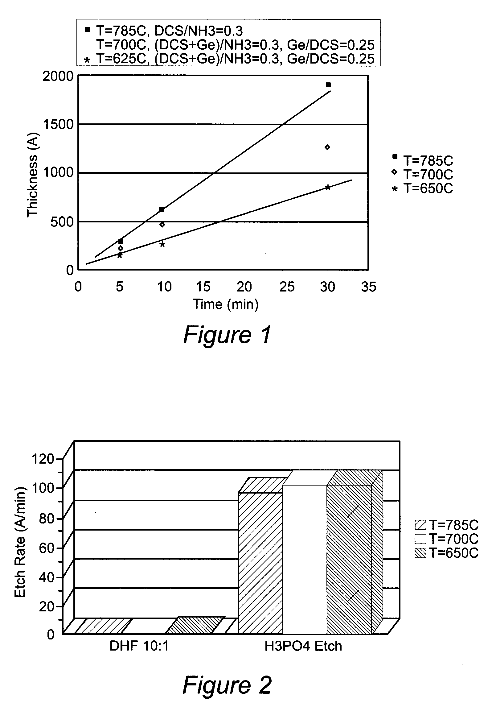
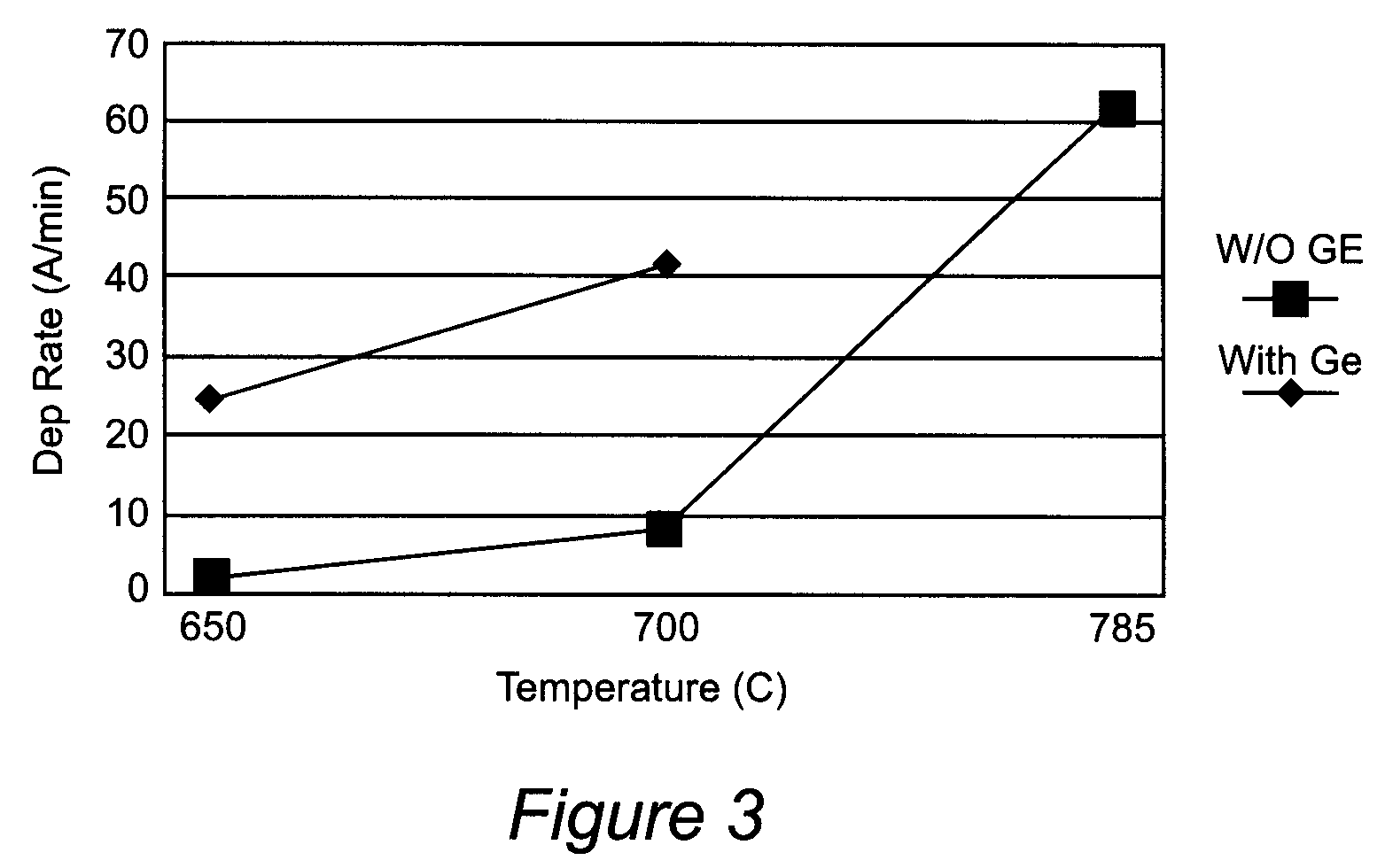
[0043] In an LPCVD furnace, GEH4 was added to a mixture of DCS and NH3 at two different temperatures, 700 and 650° C. respectively. A standard silicon nitride film was also deposited at 785° C. as a control. Two germanium-doped silicon nitride films and one standard silicon nitride film were thus deposited. The results are summarized in the charts which are FIGS. 1, 2 and 3.

[0044] In FIG. 1, the top plot is for the film deposited at 785° C., with DCS / NH3=0.3 The middle plot in FIG. 1 is for the film deposited at 700° C., with (DCS+Ge) / NH3=0.3, Ge / DCS=0.25. The bottom plot in FIG. 1 is for the film deposited at 650° C., with the same ratios as for the film deposited at 700° C.

[0045] From FIG. 3, it is clear that by adding GeH4 to the process gas, a significant increase in the deposition rate has been achieved. Also, the germanium-doped films of this Example 1 have a similar property (determined by wet etch rate) to the standard high temperature films.

[0046] The addition of germane...

example 2

[0047] Importantly, the present inventors have recognized that stress in a film may be modified by germanium addition during nitride film formation. There may be considered the following results, both for silicon substrates: (i) for a Si—N film, stress of 4 E9 Dyne / cm2 (compressive); (ii) for a SiGe—N film, stress of 8.2 E9 Dyne / cm (tensile).

[0048] As the above data shows, there is almost an order of magnitude stress difference between a conventional silicon nitride film and an inventive germanium-doped silicon nitride film.

[0049] It will be appreciated that the advantages of the present invention with regard to deposition rate and / or stress tuning are not limited to nitride films, and may be applicable for oxide films (such as silicon oxide films, etc.) and other films, such as other amorphous films.

example 3

[0050] Ge was added to a mixture of silane and ammonia, forming a Ge-doped Si nitride film. The deposition rate was increased for the germane process, compared to an equivalent no-germane process. For the no-Ge processs, the stress of the produced film was 0.4 GPa (compressive). For the inventive process using Ge, the stress was 0.8 GPa (tensile). Thus, the use of Ge according to the invention achieved a change in stress of 1.2 GPa, which was a substantial improvement.


PUM

PropertyMeasurementUnit
temperatureaaaaaaaaaa

Abstract

Adding at least one non-silicon precursor (such as a germanium precursor, a carbon precursor, etc.) during formation of a silicon nitride, silicon oxide, silicon oxynitride or silicon carbide film improves the deposition rate and / or makes possible tuning of properties of the film, such as tuning of the stress of the film. Also, in a doped silicon oxide or doped silicon nitride or other doped structure, the presence of the dopant may be used for measuring a signal associated with the dopant, as an etch-stop or otherwise for achieving control during etching.

Description

BACKGROUND OF INVENTION [0001] The present invention generally relates to films used in manufacture of semiconductor devices, especially to nitride films and oxide films. [0002] In order to improve drive current in complementary metal oxide semiconductor (CMOS) devices, stressed films have been used either as spacers or middle-of-the-line (MOL) liners (also known as pre-metal dielectric (PMD) liners). Deposition regimes that result in either highly tensile or highly compressive nitride films are well known (e.g., rapid thermal chemical vapor deposition (RTCVD), plasma enhanced chemical vapor deposition (PECVD), high density plasma (HDP) using silicon (Si) precursor such as silane (SiH4), di chloro silane (DCS), Disilane, Hexachlorodisilane, bis-tertiary butyl amino silane (BTBAS), and ammonia (NH3)). However, within a given deposition regime it only has been possible to modulate the stress within a small range. It has been very difficult to modulate the stress to a large extent with...

Claims


Application Information

Patent Timeline
Patent Type & Authority Applications(United States)
IPC IPC(8): C23C16/30C23C16/34C23C16/40H01L21/314H01L21/316H01L21/318H01L21/336H01L21/768H01L29/786
CPCC23C16/308H01L29/78675C23C16/401H01L21/0214H01L21/0217H01L21/02271H01L21/3143H01L21/3144H01L21/3145H01L21/3148H01L21/31608H01L21/31612H01L21/3185H01L21/76801H01L21/76829H01L21/76834H01L29/7833H01L29/7843C23C16/34
Inventor CHAKRAVARTI, ASHIMA B.HOLT, JUDSONCHAN, KEVIN K.DESHPANDE, SADANAND V.JAGANNATHAN, RANGARAJAN
Owner GLOBALFOUNDRIES INC
Why Eureka
Try Eureka