

Device for performing cell assays
a cell assay and cell technology, applied in the field of cell assay devices, can solve the problems of relatively limited types of cell-based assay devices, and the development of cellular assay techniques for studying electrically active cells such as myocytes, mast cells or neurons, and the functionalities are relatively low
- Summary
- Abstract
- Description
- Claims
- Application Information
AI Technical Summary
Benefits of technology
Problems solved by technology
Method used
Image

Examples
example 1
Device Fabrication
[0090] Positive photoresist (product name S1818) was photolithographically patterned on a microscope glass coverslip (22×64 mm, thickness No. 1, 0.13-0.17 mm) using electron-beam written chromic masks. A layer of titanium (10 nm) and a second layer of gold (100 nm) were evaporated on top of the patterned glass surface. Subsequent removal of the Ti / Au covered layer of the positive photoresist left behind on the glass 20 μm wide Ti / Au parallel line precursor electrodes 200 μm apart from each other and each line having at one end a bonding pad.
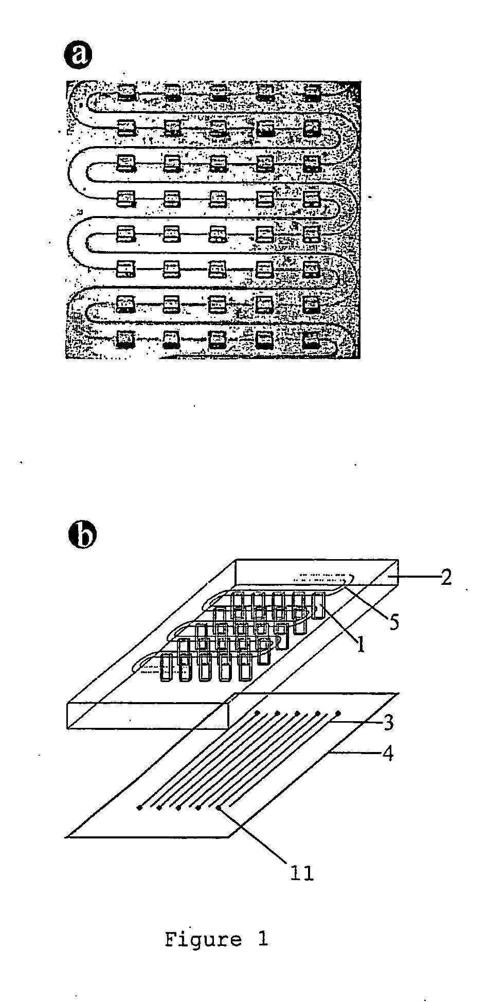
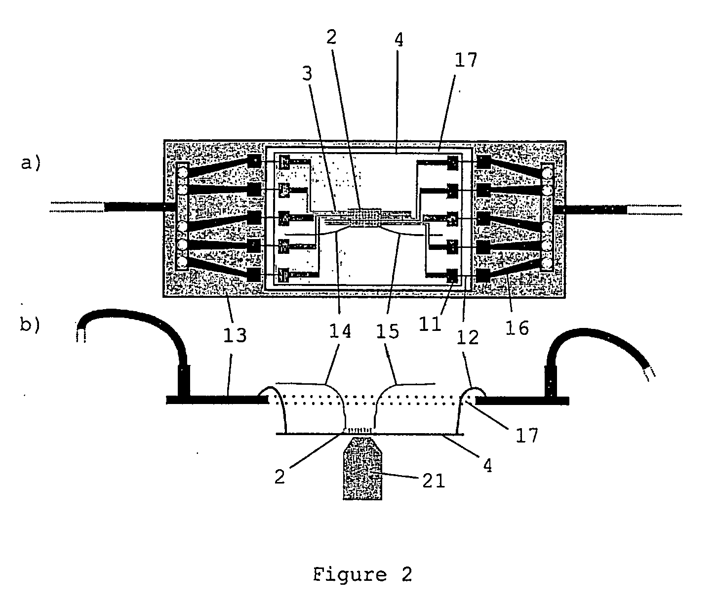
[0091]FIG. 1b shows schematically the microscope glass coverslip 4 with electrode lines 3 and bonding pads 11, and FIGS. 2a and b respectively show schematic top and side views of an assembled device which incorporates the coverslip of FIG. 1b.
[0092] The bonding pads 11 were connected with 200 μm thick gold wire 12 to the copper electrodes 16 of a printed circuit board (PCB) 13 with a central rectangular window 17 to allow t...
example 2
Device Fabrication
[0127] Microscope glass coverslips (24×40 mm, thickness No. 1, 0.13-0.17 mm) were used as substrates to allow the recording of the intra- and extracellular fluorescence as well as cellular morphology with oil and water immersion lenses (thereby enabling the use of lenses with a high numerical aperture and a low working distance of −300 μm). The device microfabrication process is shown schematically in FIGS. 11a and b.
[0128] The patterns for microelectrodes and for the walls of micron-sized elongate chambers (i.e. confinement cavities) were both designed using AutoCAD and were produced as two chrome coated maskplates, using a Philips electron beam writer. To photolithographically pattern the microelectrode array, the coverslips (FIG. 11a(i)) were first spin-coated with the thin positive photoresist S1818 at 4000 rpm, baked in the oven at 90° C. for 30 min with an intermediate 15 min soak in chlorobenzene, and were then exposed to UV-light, through the appropriate...
PUM
| Property | Measurement | Unit |
|---|---|---|
| Length | aaaaa | aaaaa |
| Fraction | aaaaa | aaaaa |
| Volume | aaaaa | aaaaa |
Abstract
Description
Claims
Application Information