Spin-injection device and magnetic device using spin-injection device

a technology of injection device and magnetic device, which is applied in the direction of superconductor device, radio frequency controlled device, instrument, etc., can solve the problems of reduced magnetic switching field, insufficient signal voltage, and small detection output resistance, so as to achieve large signal voltage, large resistance change, and large output resistance

Inactive Publication Date: 2006-02-02
JAPAN SCI & TECH CORP
View PDF5 Cites 33 Cited by
  • Summary
  • Abstract
  • Description
  • Claims
  • Application Information

AI Technical Summary

Benefits of technology

[0020] So constructed as mentioned above, according to the present invention, the spin injection device, which uses any one of a semiconductor, a semimetal and a superconductor that is smaller in carrier density than a nonmagnetic metal, can provide an markedly larger output resistance Rs derived from spin accumulation than that of the conventional spin injection device which is made of metal as the nonmagnetic conductor. Further, it can provide a large signal voltage by virtue of a large resistance change accompanied in the spin injection with low current and under low magnetic field. Furthermore, a spin injection device can be provided that can be miniaturized in its size while permitting low magnetic switching field even under low magnetic field.

Problems solved by technology

In the conventional spin injection device in which the nonmagnetic metal 53 as the common electrode has small resistance, the problem arises that the detected output resistance is as small as 10 m Ω and fails to provide a practically sufficient signal voltage.
Thus, the conventional spin injection device has the problem that the magnetic switching field increases when reduced in size.
And it can not be operated under the low magnetic field.
This requires that a large current should be flown with a wire separately provided in the MRAM to generate sufficient external field, thus incurring an increase of power consumption.
Consequently, there has been the problem that limitations are brought about in increasing the storage capacity, e.g., from the fact that reducing magnetic switching field requires increasing the device area in a tunnel junction.

Method used


Image

  • Spin-injection device and magnetic device using spin-injection device
  • Spin-injection device and magnetic device using spin-injection device
  • Spin-injection device and magnetic device using spin-injection device

Examples


example 1

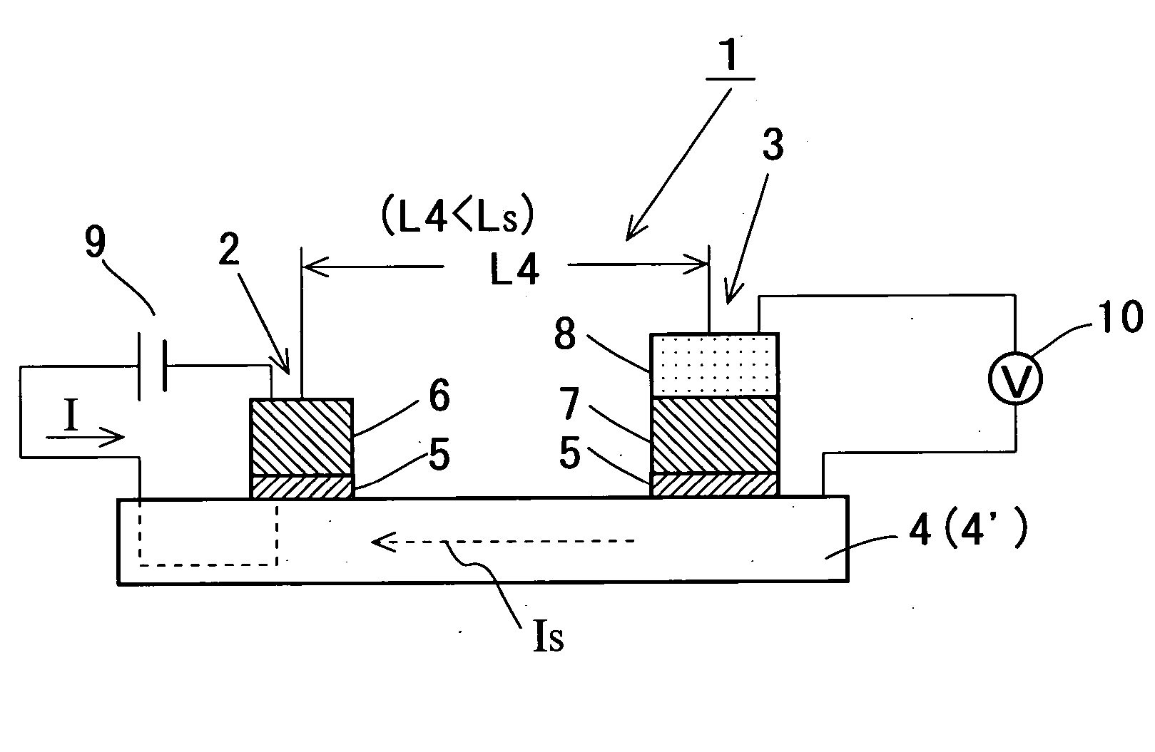
[0053] A spin injection device 1 (FIG. 1) that implements the present invention was made as follows. The GaAs film doped by Si (silicon) as an impurity was epitaxially grown to having a thickness of 100 nm onto a semi-insulating GaAs substrate 11 to form the nonmagnetic conductor 4 by using MBE (molecular beam epitaxy).

[0054] The Al film having a thickness 1.2 nm was deposited onto the GaAs thin film. This Al film was oxidized using plasma oxidation to form an Al oxide film as the insulator 5. Thereafter, Co was deposited to a film thickness of 3 nm to form the ferromagnet 7 onto the Al oxide film, and then IrMn was deposited to a film thickness of 10 nm to form the antiferromagnet 8.

[0055] The multilayered film mentioned above was miniaturized using electron beam lithography and Ar ion milling to fabricate a structure as typically shown in FIG. 1 in which the Si doped GaAs film serves as the nonmagnetic conductor 4 for two tunnel junctions 2 and 3. The Si doped GaAs film had a wi...

example 2

[0058] A spin injection device 1 (FIG. 1) that implements the present invention was made as follows. The substrate 11 was a Si substrate covered with a thermally oxidized film on which substrate a thin metal film of Nb (niobium) having a thickness of 100 nm was deposited using an ultrahigh vacuum sputtering apparatus to form the superconductor 4′. The Al was deposited to a film thickness of 1.5 nm onto the Nb thin film. This Al film was oxidized using plasma oxidation to form an Al oxide film as the insulator 5. Thereafter, Co90Fe10 alloy was deposited to a film thickness of 5 nm to form the ferromagnet 7 onto the Al oxide film, and then IrMn was deposited to a film thickness of 10 nm to form the antiferromagnet 8.

[0059] The multilayered film mentioned above was miniaturized using electron beam lithography and Ar ion milling to fabricate a structure as typically shown in FIG. 1 in which the Nb thin film serves as the nonmagnetic conductor 4 for two tunnel junctions 2 and 3. The Nb ...

example 3

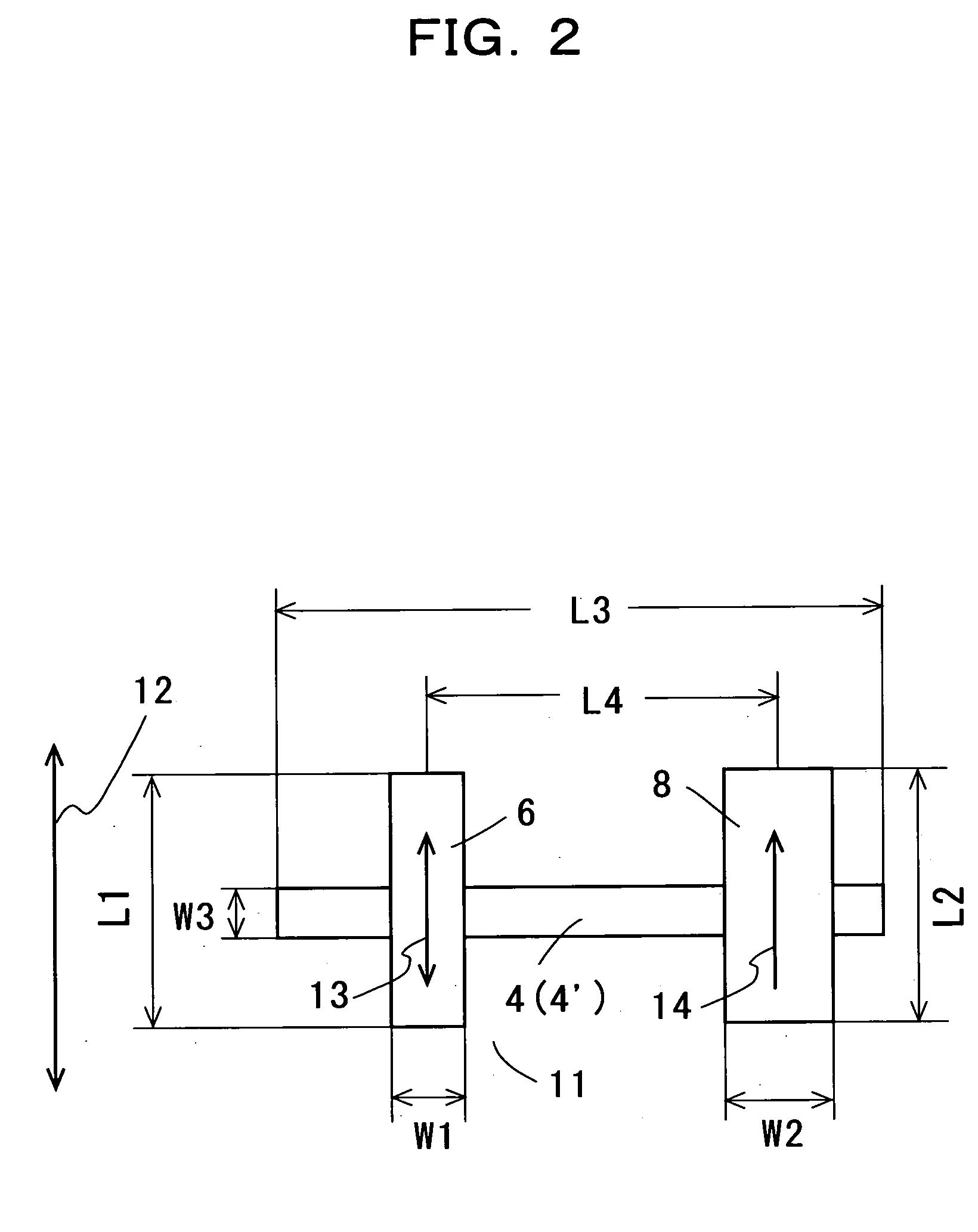
[0062] A spin injection device 20 that implements the present invention was made as follows. This Example is the same as Example 2 except that in the first tunnel junction 2 the Co90Fe10 alloy film in Example 2 was replaced by a three layers film made of Co90Fe10 of 5 nm thick, Ru of 0.45 nm thick and Co90Fe10 of 3 nm thick. And, the spin injection device 20 prepared had ferromagnets 23 and 25 magnetically coupled antiparallel to each other via a nonmagnetic metal 24 in each of the first and second tunnel junctions 21 and 22 as shown in FIG. 3. In the course of this fabrication, it was confirmed that the two Co90Fe10 ferromagnets were magnetically coupled antiparallel to each other via Ru in the layered structure of Co90Fe10 (5 nm), Ru (0.45 nm) and Co90Fe10 (3 nm).

[0063] In the spin injection device 20 of the present invention so prepared, the current I flowed, at a temperature of 1.5 K, from the Co90Fe10 (5 nm) / Ru (0.45 nm) / Co90Fe10 (3 nm) film via the Al oxide film to the Nb thi...


PUM

PropertyMeasurementUnit
aspect ratioaaaaaaaaaa

Abstract

A first and a second tunnel junctions (2 and 3) which have a common electrode composed of a nonmagnetic conductor (4) and each of which has a counterelectrode composed of a ferromagnet (6, 8) are disposed spaced apart from each other by a distance that is shorter than a spin diffusion length of the nonmagnetic conductor (4) wherein the first tunnel junction (2) acts to inject spins from the ferromagnet (6) into the nonmagnetic conductor (4) and the second tunnel junction (3) serves to detect, between the ferromagnetic metal (8) and the nonmagnetic conductor (4), a voltage that accompanies spin injection of the first tunnel junction (2) and wherein the nonmagnetic conductor (4) is a nonmagnetic conductor, such as a semiconductor or a semimetal, that is lower in carrier density than a metal. The common electrode alternatively may be composed of a superconductor (4′). A spin injection device thus provided can exhibit a large signal voltage with low current and under low magnetic field and can be miniaturized in device size. Magnetic apparatuses utilizing such a spin injection device are also provided.

Description

TECHNICAL FIELD [0001] The present invention relates to a spin injection device and a magnetic apparatus using the same. BACKGROUND ART [0002] The magnetoresistance effect that when an external magnetic field is applied to a metal or semiconductor, a change is produced in its resistivity has been utilized in magnetic heads and sensors. To obtain larger magnetoresistance, a magnetoresistance device using a tunnel junction is available, of which the ferromagnetic spin tunnel junction (MTJ) device and the spin injection device have drawn attention. In recent years, the attention has been focused on a magnetoresistance device using the tunnel junction as a new magnetic sensor or a new memory device for a magnetic random access memory (MRAM). [0003] The conventional MTJ device has a ferromagnetic spin tunnel junction made of a layered structure having a ferromagnetic, an insulating and a ferromagnetic layer deposited in this order. When an external magnetic field is applied to control ma...

Claims


Application Information

Patent Timeline
Patent Type & Authority Applications(United States)
IPC IPC(8): H01L29/76H01L43/00G01R33/06G01R33/09G11B5/39H01L21/8246H01L27/105H01L39/22H01L43/08H01L43/12
CPCB82Y10/00B82Y25/00G01R33/06G11B5/39G11B5/3903Y10T428/1193H01L29/66984H01L39/228H01L43/08Y10T428/1121Y10T428/1143G11B5/3909H10N60/128H10N50/10G11C11/15G11C11/16H10B61/00
Inventor INOMATA, KOUICHIROMAEKAWA, SADAMICHITAKAHASHI, SABURO
Owner JAPAN SCI & TECH CORP
Why Eureka
Try Eureka