Thin film transistor and method for fabricating same

a thin film transistor and fabrication method technology, applied in the direction of transistors, semiconductor devices, electrical equipment, etc., can solve the problems of excessive electrical leakage, serious problems, and the fabrication method of the thin film transistor according to the prior art often produces a serious problem, and achieves enhanced characteristics and functionality of the amorphous silicon layer and the gate insulation layer, and improves the interface. the effect of good performan

Active Publication Date: 2006-02-02
AU OPTRONICS CORP
View PDF10 Cites 49 Cited by
  • Summary
  • Abstract
  • Description
  • Claims
  • Application Information

AI Technical Summary

Benefits of technology

[0019] Due to the microstructure of the microcrystalline material of interface layer, various factors including the size of the grains, the void ratio, and the crystallization ratio are easily controlled during the fabrication process. Therefore, it becomes evident that the interface layer is able to further enhance the characteristics and functionality of the amorphous silicon layer and the gate insulation layer. Consequently, not only is the carrier mobility of the thin film transistor well maintained when the thin film transistor is turned on, but also the electrical leakage is controlled within a range lesser than the thin film transistor of the prior art when the thin film transistor is turned off.
[0020] Also, due to the fact that the characteristics of the interface is well improved, the dangling bond phenomenon generated from the Si / SiNx interface of the prior art is also greatly controlled, thereby further extends the stability of the threshold voltage and life expectancy of the thin film transistor. By utilizing the present invention, the total fabrication time is likely to remain the same as the entire active layer is not deposited to become a microcrystalline silicon layer and no additional equipments are needed as the entire process can be completed via original PECVD equipments.

Problems solved by technology

Nevertheless, the fabrication method of the thin film transistor 26 according to the prior art often produces a serious problem.
Conversely, the electrical leakage also becomes excessively large when the thin film transistor 26 is turned off.
However, the method stated previously also causes other serious problems.
First, an extra excimer laser annealing step is added to the fabrication process and thereby significantly increases the overall time and cost.
Secondly, when an excimer laser annealing process is performed, numerous variables are required to be controlled simultaneously.
Typically, the quality of the active polysilicon thin film within the passageway becomes difficult to control if the fabrication process is not properly regulated.
In addition, the laser crystallization process is essentially a low temperature solid phase recrystallization process that characterizes a long processing time.
Consequently, the grains are only able to grow to a certain size and the grain size is also difficult to control.
Eventually, the overall carrier mobility and the control of electrical leakage are greatly affected.
Therefore, it becomes a great challenge to develop a fabrication process that is capable of producing a semiconductor layer containing an expected microcrystalline structure and achieving a satisfactory carrier mobility and low electrical leakage by utilizing the semiconductor layer as an active layer of a thin film transistor.

Method used


Image

  • Thin film transistor and method for fabricating same
  • Thin film transistor and method for fabricating same
  • Thin film transistor and method for fabricating same

Examples


Embodiment Construction

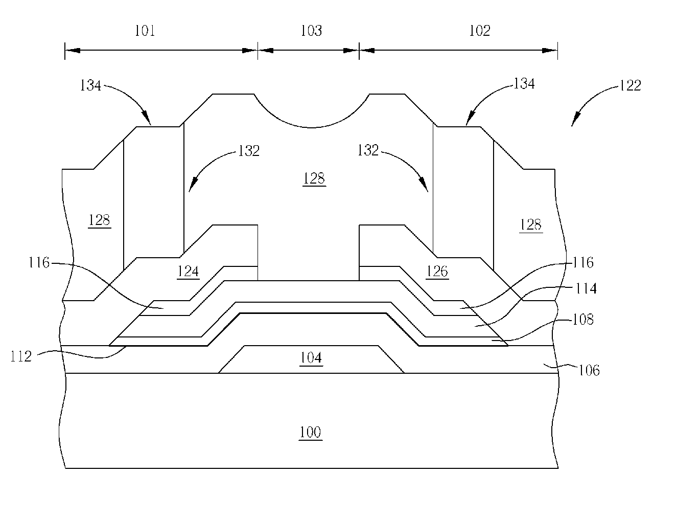
[0031] Please refer to FIG. 5 to FIG. 8. FIG. 5 to FIG. 8 are schematic diagrams of the first embodiment of the present invention for fabricating at least one thin film transistor 122. As shown in FIG. 5, the thin film transistor of the first preferred embodiment of the present invention is a bottom gate structure. The thin film transistor 122 is essentially fabricated on an insulation substrate 100. The substrate 100 is comprised of a transparent material, such as a glass substrate, a quartz substrate, or a plastic substrate. A predetermined source region 101, a predetermined drain region 102, and a predetermined channel region 103 are formed on a surface of the insulation substrate 100. A first sputtering process is performed first to form a first metal layer (not shown) on a surface of the insulation substrate 100. The first metal layer (not shown) may be a single-layered metal layer or a multi-layered metal layer. The single-layered metal layer and the multi-layered metal layer ...


PUM

PropertyMeasurementUnit
thicknessaaaaaaaaaa
gate voltageaaaaaaaaaa
source-drain voltageaaaaaaaaaa

Abstract

A method for forming a thin film transistor on a substrate is disclosed. A gate electrode and a gate insulation layer are disposed on a surface of the substrate. A deposition process is performed by utilizing hydrogen diluted silane to form a silicon-contained thin film on the gate insulation layer first. A hydrogen plasma etching process is thereafter performed. The deposition process and the etching process are repeated for at least one time to form an interface layer. Finally, an amorphous silicon layer, n+ doped Si layers, a source electrode, and a drain electrode are formed on the interface layer.

Description

BACKGROUND OF INVENTION [0001] 1. Field of the Invention [0002] The invention relates to a method for fabricating a thin film transistor and related circuits, and more particularly, to a method with improved carrier mobility and stable threshold voltage. [0003] 2. Description of the Prior Art [0004] In recent years, various display techniques have been developed flourishingly. After continuous research and development, new products such as liquid crystal displays (LCDs), plasma display panels (PDPs), and organic light emitting diode (OLED) displays have been gradually commercialized and applied to various display apparatuses with different sizes. Without any exception, all of the manufacturers today are developing toward high brightness and high efficiency for fabricating a much more commercially profitable display. Among numerous flat display techniques developed today, liquid crystal displays have been considered as one of the most mature techniques. Evidently, electronic products...

Claims


Application Information

Patent Timeline
Patent Type & Authority Applications(United States)
IPC IPC(8): H01L21/84H01L29/792H01L21/00H01L21/336H01L29/49H01L29/786
CPCH01L29/4908H01L29/78609H01L29/66765
Inventor GAN, FENG-YUANLIN, HAN-TU
Owner AU OPTRONICS CORP
Why Eureka
Try Eureka