

Organic electroluminescent element
- Summary
- Abstract
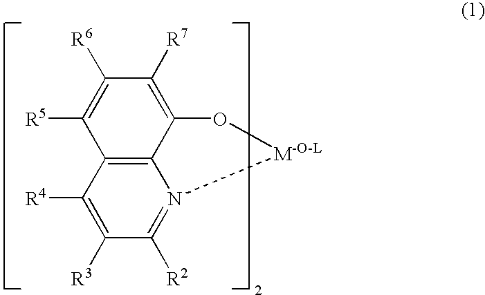
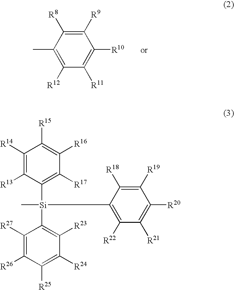
- Description
- Claims
- Application Information
AI Technical Summary
Benefits of technology
Problems solved by technology
Method used
Image

Examples
example 1
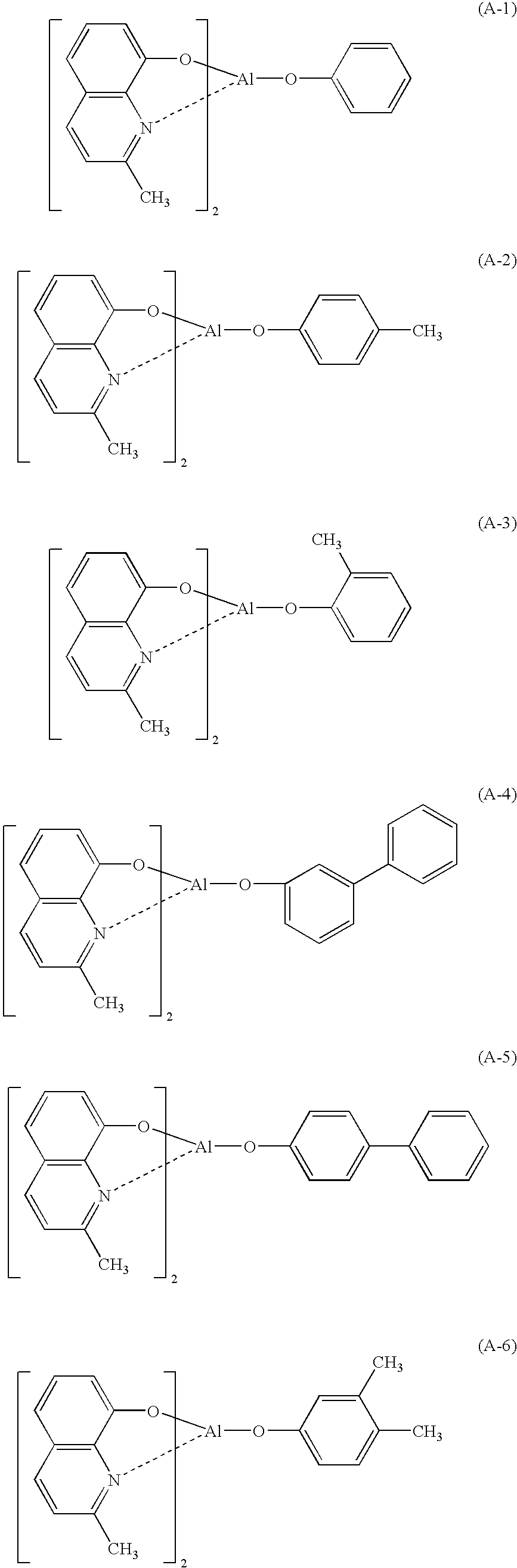
[0115] A glass substrate (manufactured by GEOMATEC Company) of 25 mm×75 mm×1.1 mm thickness having an ITO transparent electrode was cleaned by application of ultrasonic wave in isopropyl alcohol for 5 minutes and then by exposure to ozone generated by ultraviolet light for 30 minutes. The glass substrate having the transparent electrode which had been cleaned was adhered to a substrate holder of a vacuum vapor deposition apparatus. On the surface of the cleaned substrate at the side having the transparent electrode, a film of copper phthalocyanine (referred to as a film of CuPc, hereinafter) having a thickness of 10 nm was formed in a manner such that the formed film covered the transparent electrode. The formed film of CuPc worked as the hole injecting layer. On the formed film of CuPc, a film of 4,4′-bis[N-(1-naphthyl)-N-phenylamino]biphenyl shown below (referred to as a film of α-NPD, hereinafter) having a thickness of 30 nm was formed. The formed film of α-NPD worked as the hole...
example 2
[0117] An organic EL device was prepared in accordance with the same procedures as those conducted in Example 1 except that the foregoing compound (B-45) on page 45 was used for the electron injecting layer in place of the compound (A-5), and the luminance of emitted light, the efficiency of light emission and the half life were measured in accordance with the same procedures as those conducted in Example 1. The results are shown in Table 1.
example 3
[0118] An organic EL device was prepared in accordance with the same procedures as those conducted in Example 1 except that the foregoing compound (B-49) on page 45 was used for the electron injecting layer in place of the compound (A-5) and Cs was used as the reductive dopant in place of Li, and the luminance of emitted light, the efficiency of light emission and the half life were measured in accordance with the same procedures as those conducted in Example 1. The results are shown in Table 1.
PUM
| Property | Measurement | Unit |
|---|---|---|
| Time | aaaaa | aaaaa |
| Time | aaaaa | aaaaa |
| Time | aaaaa | aaaaa |
Abstract
Description
Claims
Application Information