Light-emitting device of field-effect transistor type

a field-effect transistor and light-emitting device technology, applied in the direction of semiconductor devices, basic electric elements, electrical appliances, etc., can solve the problems of reducing the efficiency of the contribution of injected carriers to light emission, emitted unnecessary wavelengths, and the foregoing problem of the reduction of light-emission property due to additives is not raised

Inactive Publication Date: 2006-03-02
HOYA CORP
View PDF7 Cites 53 Cited by
  • Summary
  • Abstract
  • Description
  • Claims
  • Application Information

AI Technical Summary

Benefits of technology

[0026] (9) A field-effect transistor type light-emitting device according to any one of (1) to (6), wherein said inorganic semiconductor material contains a group II-VI compound, or Zn and at least one element selected from S, Se, and Te.
[0027] (10) A field-effect transistor type light-emitting device according to any one of (1) to (6), wherein said inorganic semiconductor material contains a group III-V compound, or N and at least one element selected from Al, Ga, and In.
[0028] (11) A field-effect transistor type light-emitting device according to (9), wherein said inorganic semiconductor material further contains Mn as dopants that form luminescence centers.
[0029] (12) A field-effect transistor type light-emitting device according to (9), wherein said inorganic semiconductor material further contains, as dopants that form luminescence centers, at least one element among rare earth elements, or at least one element among Tm, Tb, Pr, and Sm.
[0030] (13) A field-effect transistor type light-emitting device according to (9), wherein said inorganic semiconductor material further contains, as dopants that form luminescence centers, at least one metal element, or at least one element among Cu, Ag, Au, Al, Ga, In, Cl, F, Br, and I.
[0031] (14) A field-effect transistor type light-emitting device according to (9), wherein said inorganic semiconductor material further contains, as dopants that form luminescence centers, at least one element among Cu, Ag, and Au, and at least one element among Al, Ga, In, Cl, F, Br, and I.

Problems solved by technology

However, in the pn-junction light-emitting diode, it is an unavoidable problem that while sufficient light emission cannot be obtained without doping a lot of additives into semiconductor materials, there occur deformation, defect, and the like in crystal structures of the semiconductor materials due to the doping of the additives, which become quenching centers or induce light emission of unnecessary wavelengths, thereby reducing the efficiency of contribution of the injected carriers to light emission.
Therefore, the foregoing problem of the reduction in light-emission property due to the additives is not raised.

Method used


Image

  • Light-emitting device of field-effect transistor type
  • Light-emitting device of field-effect transistor type

Examples


example 1

Example of Diamond Single Crystal

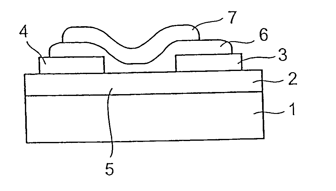
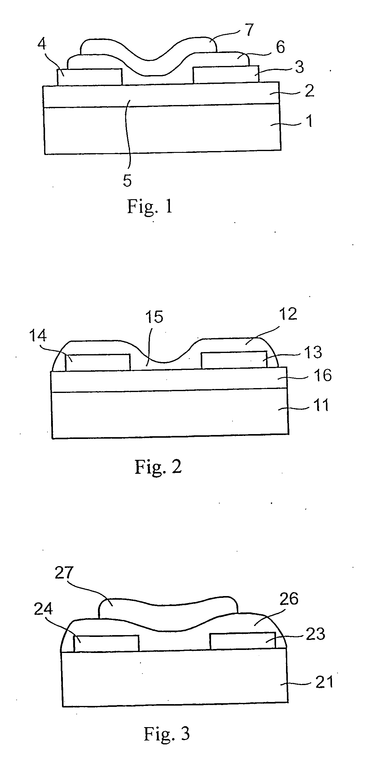
[0139] As the substrate shown in FIG. 1, preparation was made of a high-pressure / high-temperature synthetic Ib type diamond single crystal having a plate-like shape with the surface being a square with a side of 2 mm and with a thickness of 0.2 mm.

[0140] The surface of the diamond substrate was formed by mechanically surface-polishing a {100} facet of the diamond crystal. The misorientation angle thereof was 0.5°. This crystal diamond substrate was subjected to ultrasonic washing using isopropanol and acetone in order, then immersed into a chromic acid solution with simultaneous application of ultrasonic wave, then further subjected to a so-called RCA washing process to remove adsorbed substances.

[0141] Then, an undoped homoepitaxial diamond film was formed on the diamond substrate as the emission activated member by the use of the microwave plasma chemical vapor deposition (hereinafter, MW-PCVD) method. The washed diamond substrate was attached t...

example 2

Example of Amorphous Carbon

[0162] Preparation was made of a substrate made of synthetic quartz glass and having a square shape with a side of 2 mm and a thickness of 0.2 mm. The substrate surface was mechanically surface-polished, and the average roughness was Ra=5 nm. An RCA washing process like in Example 1 was applied to the substrate to thereby remove adsorbed substances.

[0163] Then, an undoped amorphous carbon hydride (a-C:H) layer was formed as an emission active member on the substrate by the plasma chemical vapor deposition (hereinafter, rf-PCVD) method. The washed quartz substrate was attached to a conductive substrate holder provided in a film forming chamber of an rf-PCVD apparatus, and super-high evacuation (background pressure: 8×10⁻⁶ Pa) was carried out. This rf-PCVD apparatus has a structure wherein a high frequency of 13.56 MHz produced from an oscillator is inputted via an impedance matching device into one end of a helical antenna with a pitch of 1.5 cm and 5 tur...

example 3

Example of ZnS:Cu,Al

[0174] On an Si (p-type; resistivity: 8 Ωcm) substrate having a size of 15×15 mm and a thickness of 650 μm and having on the surface thereof a thermally oxidized film of 200 nm as an insulator, a source electrode and a drain electrode each having a size of 1 mm×2 mm and a thickness of 80 nm were disposed at an interval of 20 μm therebetween (with sides of 2 mm facing each other) by the high-frequency sputtering method using Au as an electrode material.

[0175] Further, ZnS:Cu,Al as an emission active member was stacked thereon by electron-beam deposition. The film formation was carried out at a substrate heating temperature of 250° C. by the use of a ZnS pellet having a Cu concentration of about 0.1 mol % and an Al concentration of about 0.3 mol %, respectively, as a deposition source. The film thickness was set to 500 nm. The formed film contained 0.08 mol % of Cu and 0.26 mol % of Al.

[0176] In the formed ZnS:Cu,Al layer, the mobility of electrons was 12 cm2 / V·...


PUM


Abstract

A theme is to provide a field-effect light-emitting device that can obtain a long-term reliability and broaden a selectivity of emission wavelength. The invention of this application is a field-effect transistor type light-emitting device having an electron injection electrode, i.e. a source electrode, a hole injection electrode, i.e. a drain electrode, an emission active member disposed between the source electrode and the drain electrode so as to contact with both electrodes, and a field application electrode, i.e. a gate electrode, for inducing electrons and holes in the emission active member, which is disposed in the vicinity of the emission active member via an electrically insulating member or an insulation gap. The emission active member is made of an inorganic semiconductor material having both an electron transporting property and a hole transporting property.

Description

TECHNICAL FIELD [0001] The present invention relates to a light-emitting device using semiconductors and, more specifically, relates to a field-effect transistor type light-emitting device. BACKGROUND ART [0002] Conventionally, light-emitting devices using semiconductors have been widely used for display and illumination and as light sources. [0003] As one of such light-emitting devices, there is a light-emitting diode wherein, by applying a forward voltage to pn-junction semiconductors, electrons are injected into an n-region and holes are injected into a p-region so that light emission is achieved by recombination of electrons and holes at a junction (active region). [0004] The pn-junction of the light-emitting diode is formed by joining together a p-type semiconductor and an n-type semiconductor each produced by doping into a semiconductor an additive that forms p-type or n-type. For example, as such a pn-junction light-emitting diode, a light-emitting diode using a diamond singl...

Claims


Application Information

Patent Timeline
Patent Type & Authority Applications(United States)
IPC IPC(8): H01L33/00
CPCH01L33/0041H01L2924/0002H01L2924/00
Inventor HIROSHI, KAWAZOEKOBAYASHI, SATOSHITANI, YUKIYANAGITA, HIROAKI
Owner HOYA CORP
Why Eureka
Try Eureka