

Semiconductor device and manufacturing method thereof
- Summary
- Abstract
- Description
- Claims
- Application Information
AI Technical Summary
Benefits of technology
Problems solved by technology
Method used
Image

Examples
first embodiment
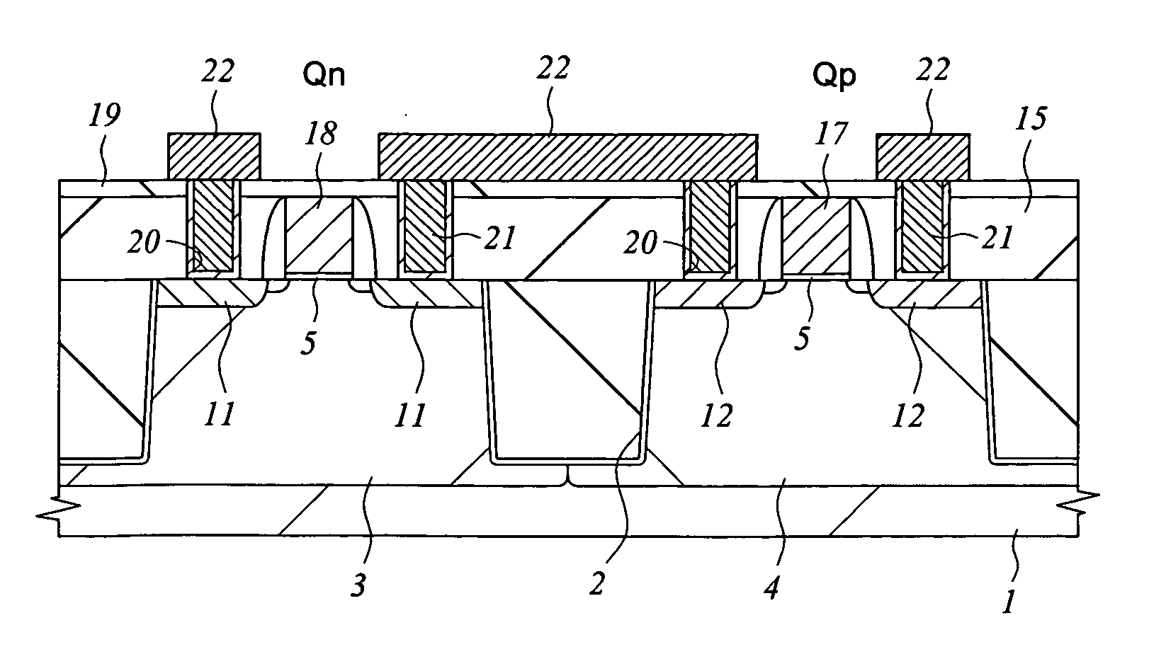
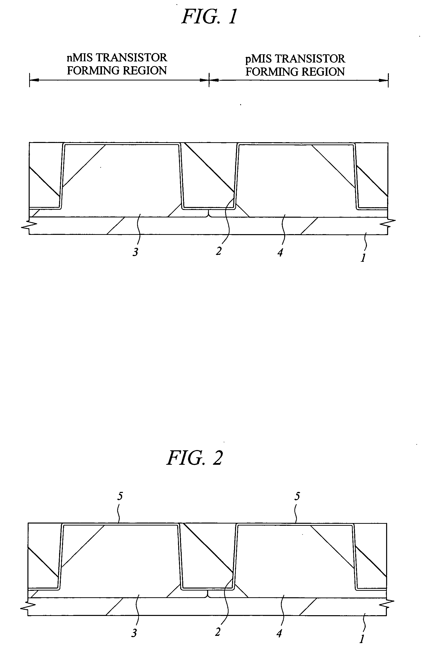
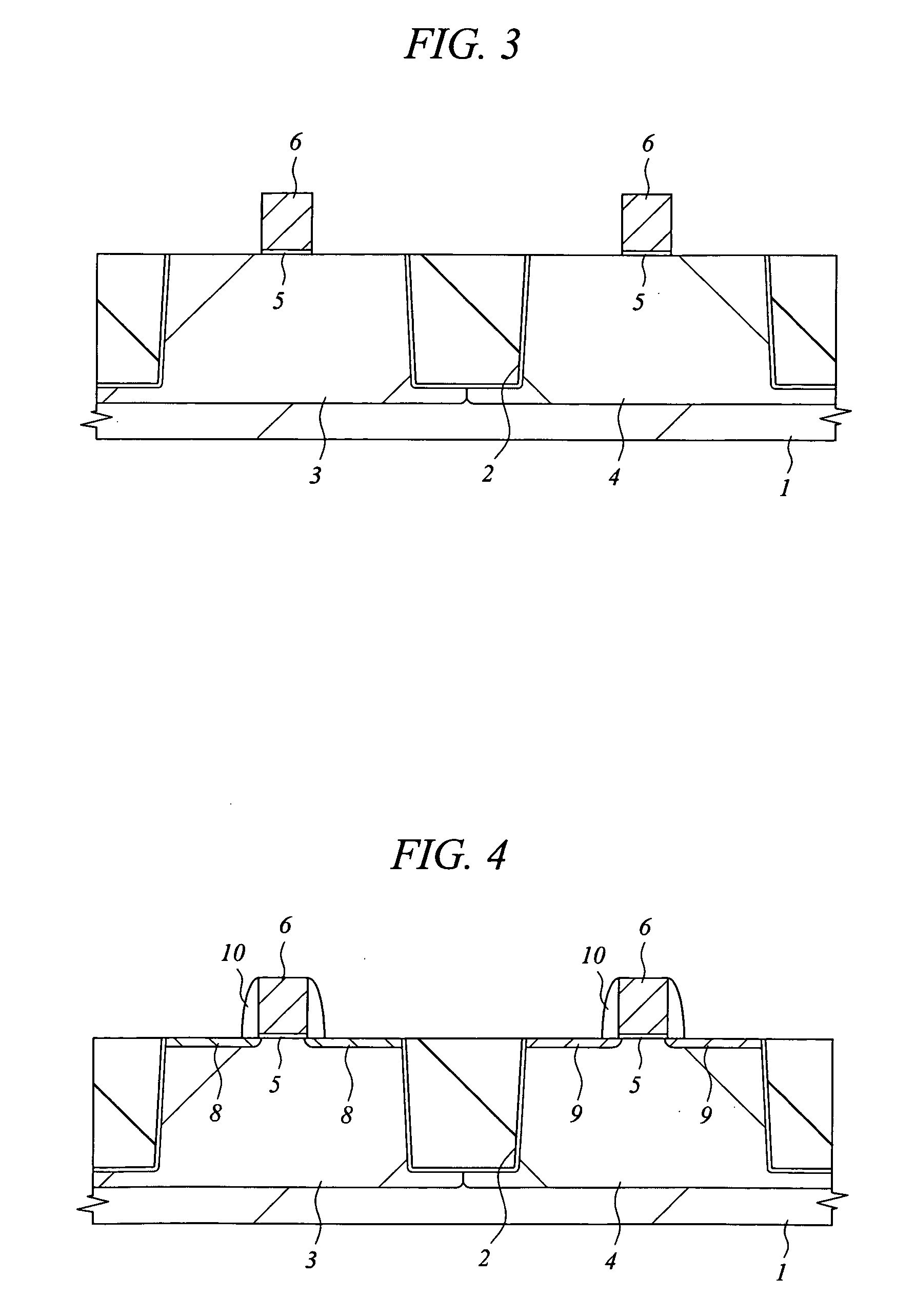
[0063] The manufacturing method of a n channel MIS transistor and a p channel MIS transistor according to the first embodiment will be described with reference to FIG. 1 to FIG. 14.
[0064] First, as shown in FIG. 1, a device isolation trench 2 is formed in the main surface of the semiconductor substrate (hereinafter, referred to as substrate) 1 made of p type single crystal silicon by using the well-known STI (Shallow Trench Isolation) technology. Thereafter, boron is ion-implanted into a n channel MIS transistor forming region of the substrate 1, and phosphorus is ion-implanted into a p channel MIS transistor forming region of the substrate 1. Subsequently, the impurities (boron and phosphorus) are diffused in the substrate by the thermal treatment of the substrate 1, thereby forming a p type well 3 and a n type well 4 in the main surface of the substrate 1.
[0065] Next, impurities for adjusting the threshold voltage of the MIS transistors are ion-implanted into the respective surf...
second embodiment
[0088] The manufacturing method of a n channel MIS transistor (Qn) and a p channel MIS transistor (Qp) according to the second embodiment will be described with reference to FIG. 15 to FIG. 25.
[0089] First, by the same method as described in the first embodiment with reference to FIG. 1, the device isolation trenches 2, the p type well 3 and the n type well 4 are formed in the main surface of the substrate 1. Subsequently, impurities for adjusting the threshold voltage of the MIS transistors are ion-implanted into the surfaces of the p type well 3 and the n type well 4. Next, as shown in FIG. 15, a gate insulator 30 made of silicon oxide is formed on each of the surfaces of the p type well 3 and the n type well 4 by the thermal treatment of the substrate 1.
[0090] Next, as shown in FIG. 16, after depositing a polycrystalline silicon film (or amorphous silicon film) on the substrate 1 by the CVD, the polycrystalline silicon film is patterned by the dry etching using a photoresist fi...
PUM
 Abstract
Description
Claims
Application Information