Method of manufacturing a capacitor
- Summary
- Abstract
- Description
- Claims
- Application Information
AI Technical Summary
Benefits of technology
Problems solved by technology
Method used
Image

Examples
example 1
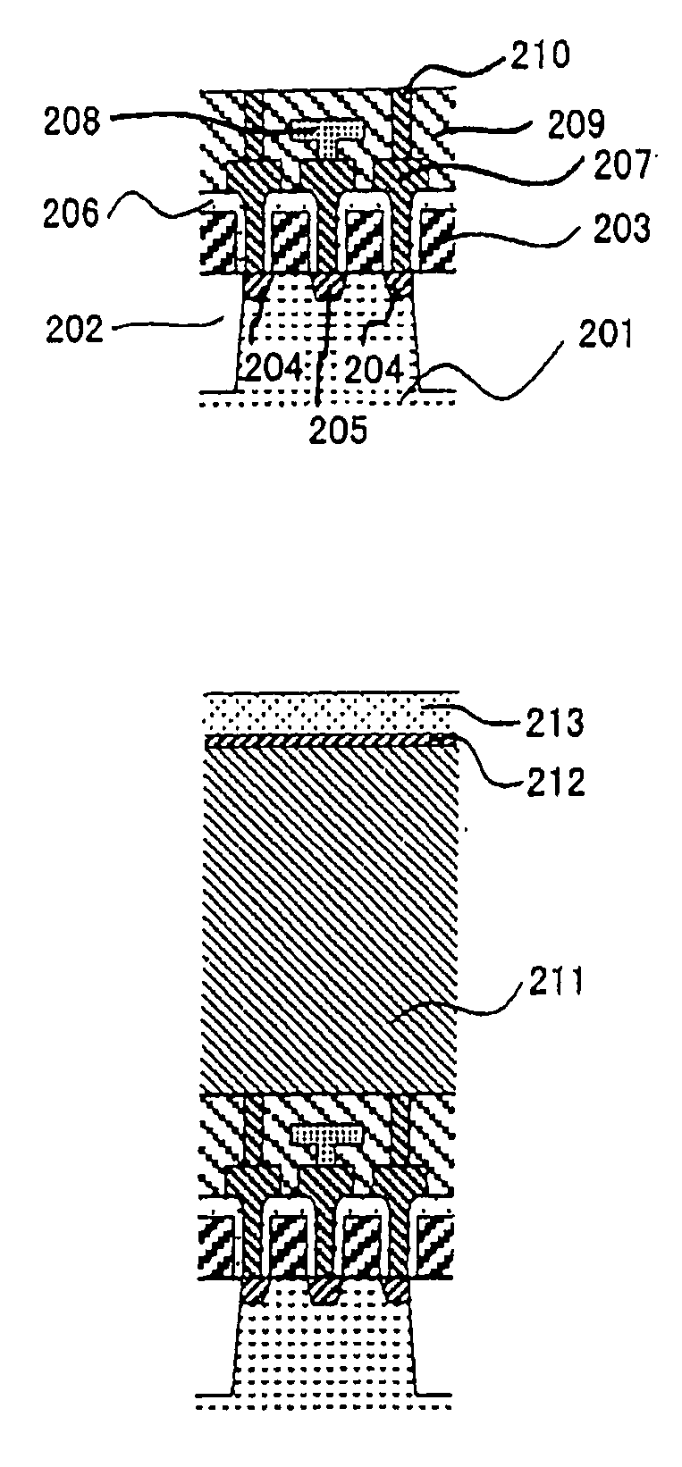
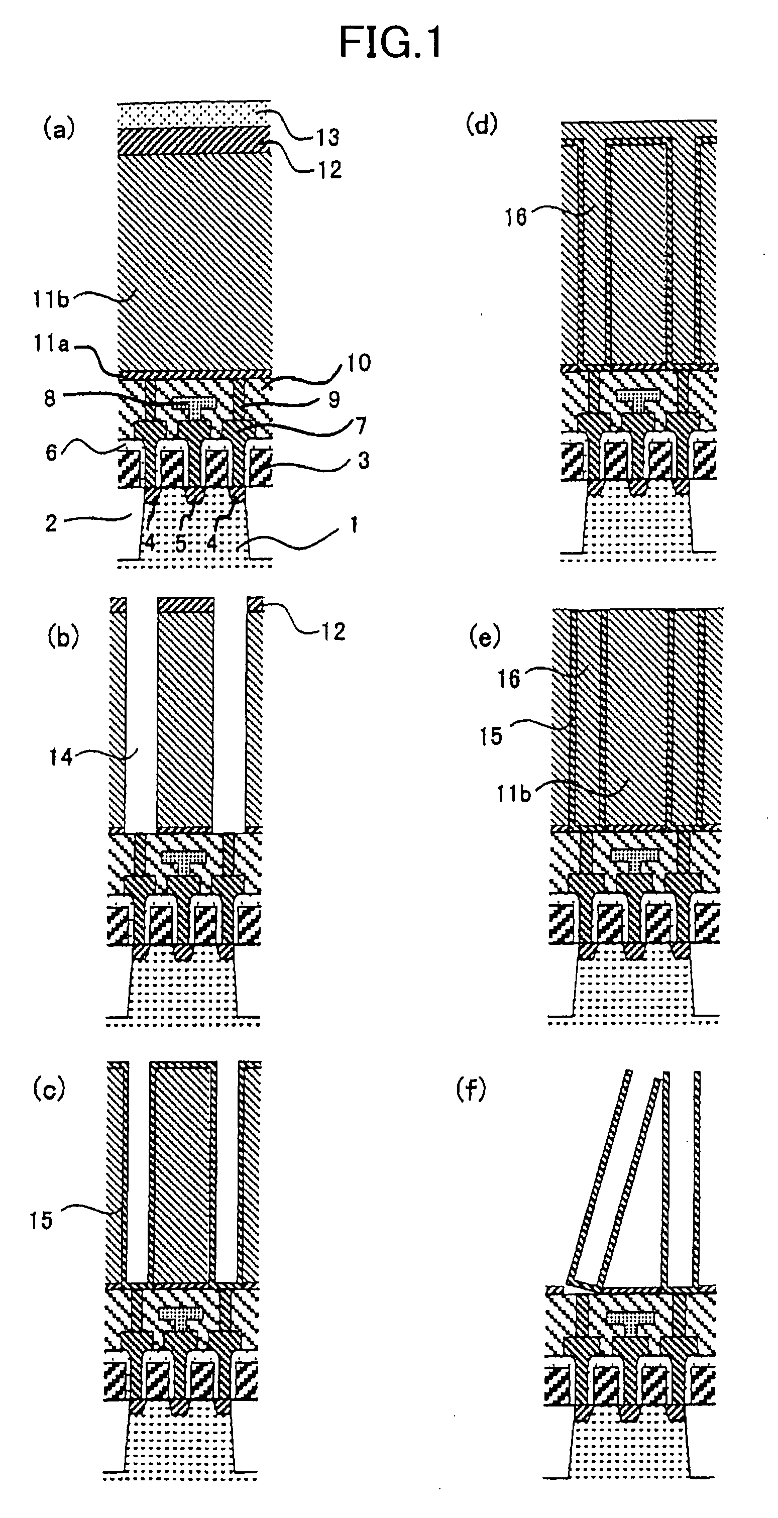
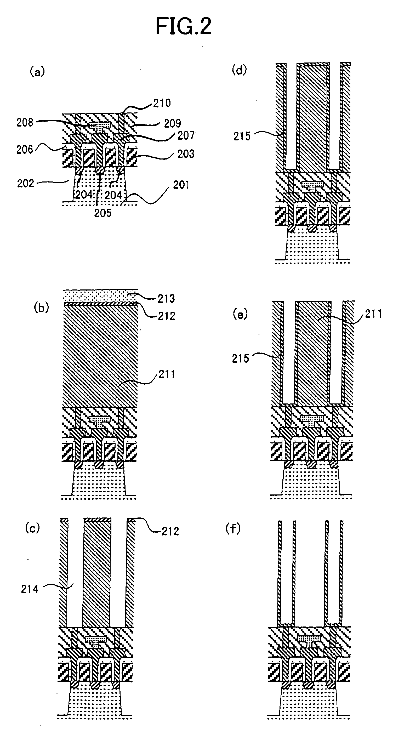
[0041] Example 1 of the invention will be described below based on accompanying drawings, with reference to a series of process cross-sectional views in FIGS. 2(a) to 2(f).
[0042]FIG. 2(a) shows a process cross-sectional view of a stage before a capacitor is formed. Device separation regions 202 were formed in predetermined areas of a p-type semiconductor board 201, and then, each gate electrode was formed through a gate insulating film (that is extremely thin and not shown in the figure) on the surface of the silicon board 201. The gate electrode constitutes a word line 203. Each insulating film 206 comprised of silicon oxide and silicon nitride was formed to coat the word line 203. Each source 205 and each drain 204 constituting a transistor were formed on the surface of the silicon board 201. Plugs 207 comprised of polysilicon were formed on the source 205 and drain 204. Further, each bit line 208 comprised of tungsten was formed on the plug 207 connected to the source 205. Then,...
example 2
[0059] Example 2 of the invention will be described below with reference to a series of process cross-sectional views in FIGS. 3(a) to 3(f). In addition, the basic process in this Example is the same as that in Example 1 described above, and redundant descriptions are omitted.
[0060]FIG. 3(a) shows a process cross-sectional view of a stage before a carbon film that is a support base material for a lower electrode is deposited.
[0061] After forming silicon oxide 309 to cover bit lines, the surface was flattened. Then, silicon nitride 310 with a thickness of 50 nm was deposited. Contact holes were formed in respective predetermined positions of the laminated film of the silicon oxide 309 and silicon nitride 310. Silicon was embedded in the contact holes to form silicon plugs 311. The silicon nitride 310 was deposited using general low-pressure CVD. Such conditions may be applied that dichlorosilane (SiH2Cl2) and ammonia is used as a material gas, the temperature is 630° C., and the pr...
example 3
[0071] Example 3 of the invention will be described below with reference to a series of process cross-sectional views in FIGS. 4(a) to 4(f). In addition, the basic process in this Example is the same as that in Example 1 or Example 2 described above, and redundant descriptions are omitted.
[0072]FIG. 4(a) shows a process cross-sectional view of a stage where each silicon plug 411 was formed in a predetermined region in silicon nitride 410 laminated on silicon oxide 409 as in Example 2.
[0073]FIG. 4(b) shows a process cross-sectional view of a stage where silicon oxide 412 with a thickness of 1000 nm was deposited subsequent to the stage in FIG. 4(a), and a carbon film 413 with a thickness of 1000 nm, silicon film 414 with a thickness of 300 nm and photoresist 415 were successively laminated and formed on the silicon oxide 412.
[0074]FIG. 4(c) shows a process cross-sectional view of a stage where each deep hole was formed in the silicon film 414 and carbon film 413.
[0075] In the sam...
PUM
 Abstract
Description
Claims
Application Information
 - Generate Ideas
- Intellectual Property
- Life Sciences
- Materials
- Tech Scout
- Unparalleled Data Quality
- Higher Quality Content
- 60% Fewer Hallucinations
Browse by: Latest US Patents, China's latest patents, Technical Efficacy Thesaurus, Application Domain, Technology Topic, Popular Technical Reports.
© 2025 PatSnap. All rights reserved.Legal|Privacy policy|Modern Slavery Act Transparency Statement|Sitemap|About US| Contact US: help@patsnap.com