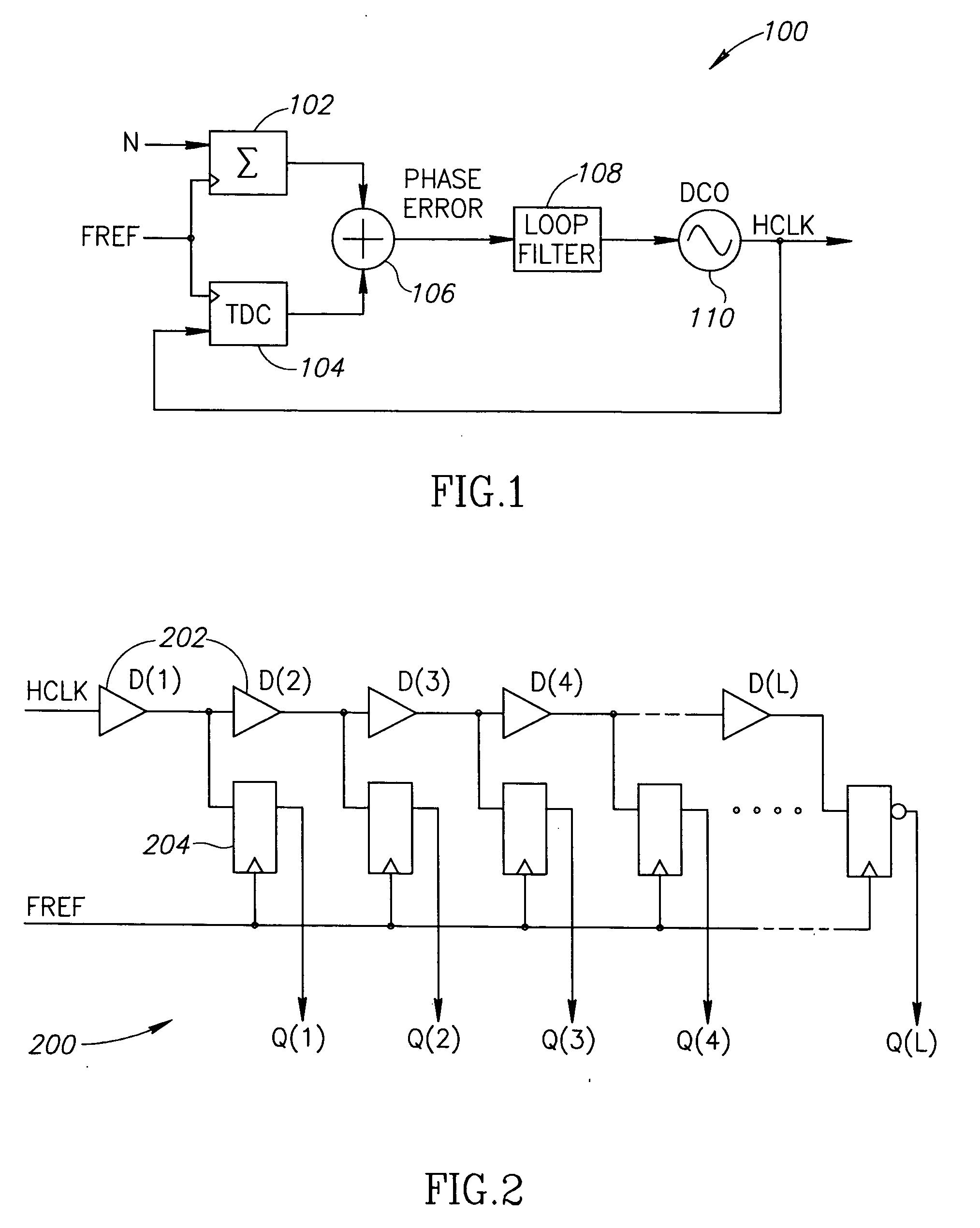
[0006] The present invention provides a solution to the problems of the prior art by providing a novel time-to-
digital converter (TDC) based on a pseudo-differential digital architecture. The TDC
circuit architecture can be used as a phase / frequency
detector and
charge pump replacement in an all-digital PLL within a
digital radio transceiver. The pseudo-differential digital architecture of the TDC circuit makes it less sensitive to NMOS and PMOS
transistor mismatches. The time conversion resolution is equal to an
inverter propagation delay, for example 15-20 ps, depending on the particular process. The
inverter propagation delay is the finest logic-level regenerative timing in
CMOS. In addition, the TDC circuit of the present invention is self-calibrating, with the
estimation accuracy better than 1%, in order to produce the output that is independent from process,
voltage and temperature variations. The output could be normalized to a period of the
high frequency clock input. The TDC circuit can also serve as a CMOS inverter
delay indicator for the purpose of inverter delay normalization, thus also providing an indication of process strength for analog circuits in large
system on
chip (SoC) dies. The TDC circuit also incorporates
power management circuitry to significantly reduce
power consumption to a very low level.
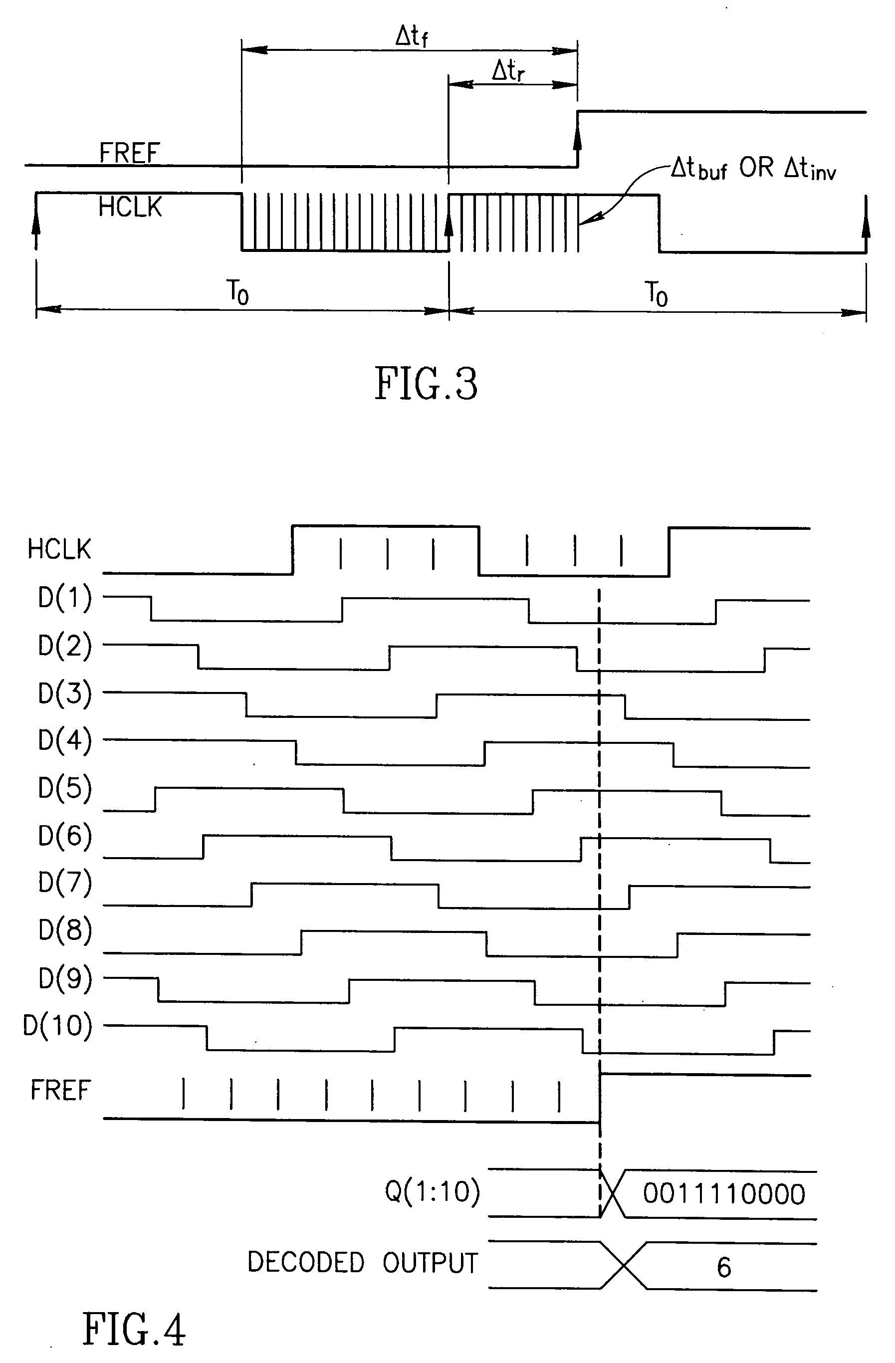
[0007] The TDC architecture of the present invention takes
advantage of the deep-submicron
CMOS process strengths of ultra-fast logic switching while avoiding its weaker handling of
voltage resolution. It is recognized that an inverter propagation delay is the finest logic-level regenerative timing method in CMOS. To this extent, the invention avoids any control of the inverter delay that would make it slower, such as using current starving techniques or increasing capacitative loads. To maximize performance, the invention also avoids fully differential structures that would require current biasing. The resolution of the TDC circuit of the present invention is the fastest possible intrinsic inverter delay (e.g., 15-20 ps in the particular
CMOS process used).
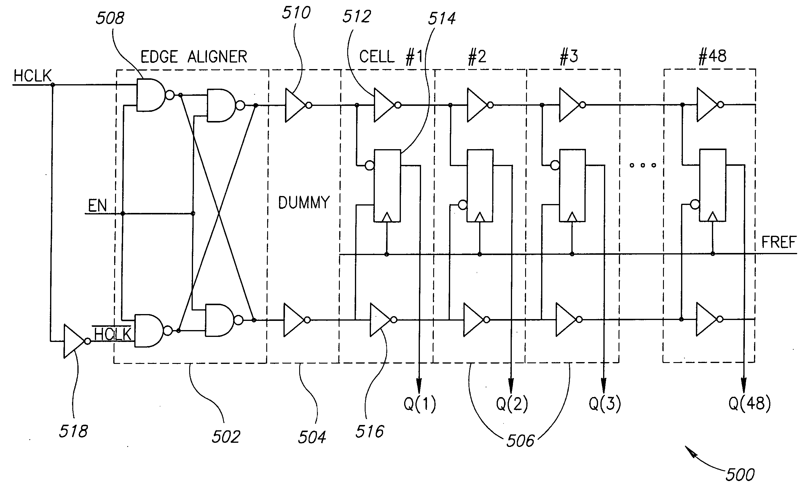
[0009] The TDC core comprises of inverters and flip-
flops and does not require any current biasing, analog interpolation or precise scaling of sub-gate delays. The architecture is based on a pseudo-differential topology that makes it less sensitive to differing strengths of NMOS and PMOS transistors. This brings the TDC resolution down to the intrinsic delay of the inverter, instead of the buffer, as in prior art designs. Taking
advantage of the availability of the two opposite phase clocks (or one
clock with an opposite phase generated internally), a novel all-digital calibration method of an inverter delay could be run during the normal operation to compensate for temperature and
voltage drifts. Since the calibration circuit reports a delay of an intrinsic, uncorrected inverter in digital form, it can be used as a
CMOS process strength indicator for process statistics and to calibrate bias current of other analog circuits on the same die. A novel power management scheme through dynamic
clock gating is applicable in PLL and other applications where the time-of arrival can be predicted. The TDC has been realized and its resolution has been measured to be as low as 17-21 ps with
integral nonlinearity (INL) of 0.7 LSB. This is achieved with very low
power consumption and area usage.
[0011] The TDC of the present invention, offers significantly better performance compared to previously known solutions: (1) 2-3 times lower
phase error in the
transmitter, (2) highly linear TDC with 30%-50% better
linearity than previous solutions, (3) 2 times improvement in resolution for phase detection, and (4) uniform performance across all channels and multiple radio bands. The above described differences contribute to a multi-band RF
transceiver supporting low
phase noise requirements for standards such as
GSM.
[0012] The advantages of the present invention include: (1) accurate phase detection with <0.5 LSB INL / DNL and high-resolution of 20 ps, (2) faster lock and PLL
settling times, (3) very low power consumption fractional phase detection circuit (less than 0.5 mW), (4) very small area (0.01 mm2) phase detection circuit, and (5)
glitch / error free TDC output digital code resulting in faster acquisition and PLL
settling times.

