

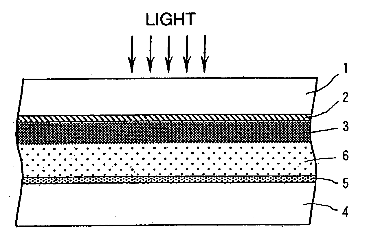
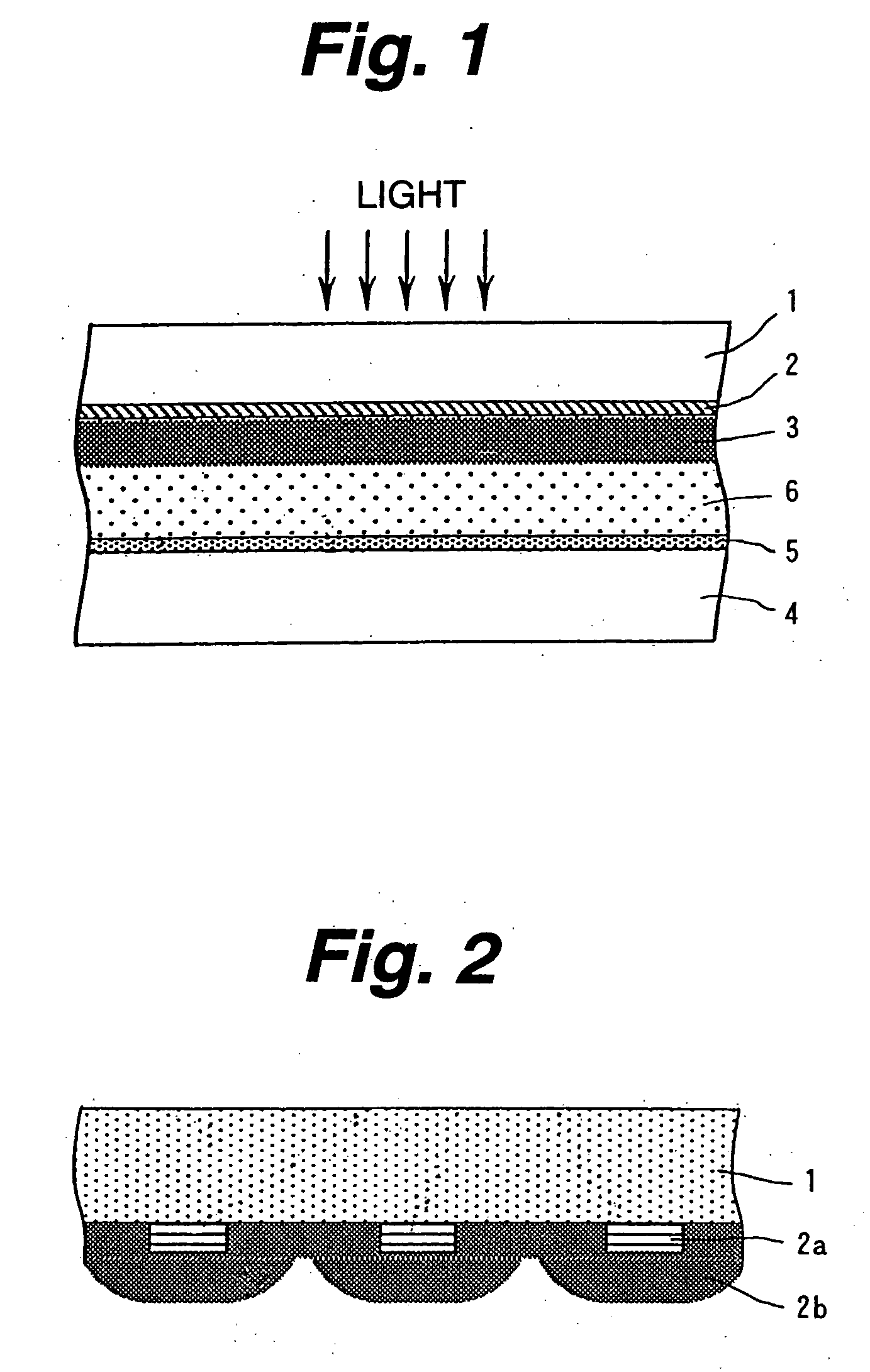
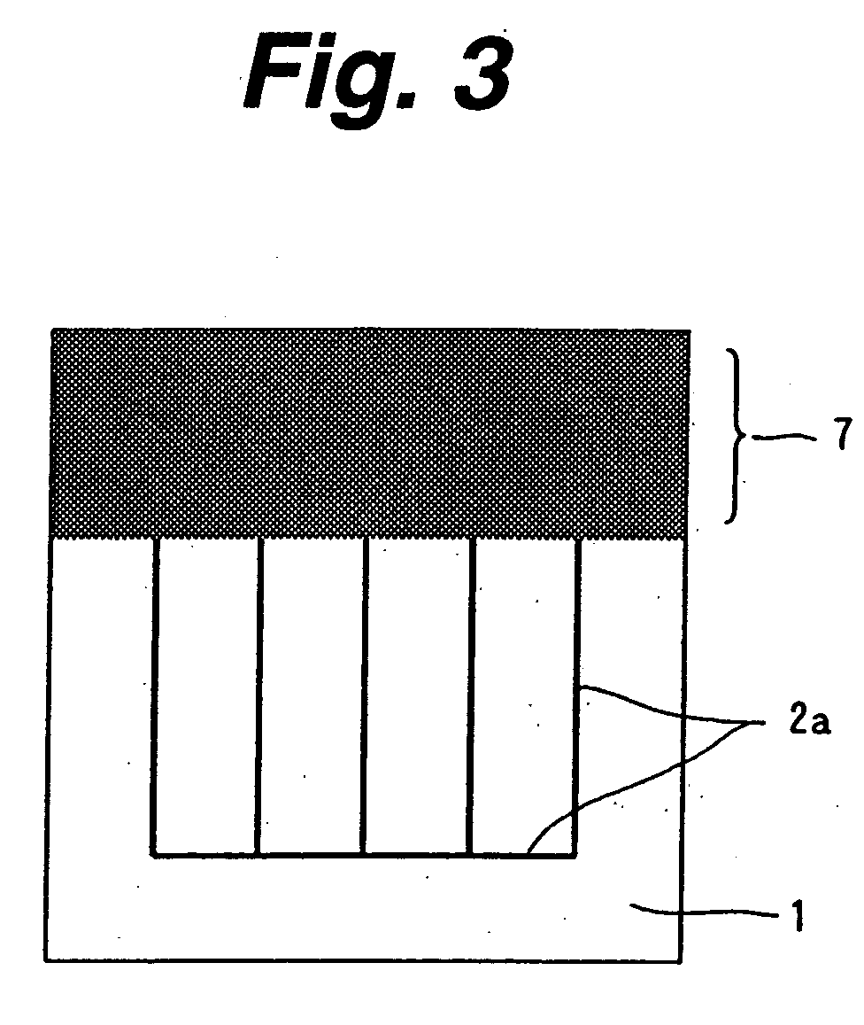
Photoelectric conversion element
a technology of photoelectric conversion element and photoelectric transfer layer, which is applied in the direction of electrolytic capacitors, pv power plants, electrochemical generators, etc., can solve the problems of difficult uniform deposit of protective layer, insufficient detection of light, and serious deformation of adhesiveness of protective layer, so as to prevent corrosion of conductive wiring layer, excellent durability and photoelectric transfer
- Summary
- Abstract
- Description
- Claims
- Application Information
AI Technical Summary
Benefits of technology
Problems solved by technology
Method used
Image

Examples
example 1
[0048] TiO2 nanoparticles were used as semiconductor nanoparticles. Referring to known methods (H. Arakawa, “Latest Techniques of Dye-sensitized Solar Cells” (C.M.C.) p. 45-47 (2001)), paste with dispersed nanoparticles was prepared as follows. 125 ml of titanium isopropoxide was seeped slowly into 750 ml of 0.1M nitric acid water solution while stirring it at the room temperature. After the seeping, the solution was moved to a constant temperature bath held at 80° C. and stirred therein for 8 hours. Thereby, Thereby, a cloudy, semi-transparent sol solution was obtained. The sol solution was left to cool down to the room temperature, then filtered through a glass filter, and 700 ml thereof was measured up. The sol solution obtained was moved to an autoclave, then annealed at 220° C. for 12 hours, and thereafter dispersed by ultrasonic treatment for one hour. Subsequently, the solution was condensed by an evaporator at 40° C. until the content of TiO2 becomes 20 wt %. The condensed s...
PUM
| Property | Measurement | Unit |
|---|---|---|
| thickness | aaaaa | aaaaa |
| thickness | aaaaa | aaaaa |
| width | aaaaa | aaaaa |
Abstract
Description
Claims
Application Information