Method for removing photoresist layer and method for forming metal line in semiconductor device using the same

a technology of photoresist layer and metal line, which is applied in the direction of photomechanical equipment, instruments, optics, etc., can solve the problems of low dielectric constant, easy oxidation of osg layer, so as to reduce the oxidation rate of low-k dielectric layer and improve device characteristics

Active Publication Date: 2006-06-15
KEY FOUNDRY CO LTD
View PDF4 Cites 17 Cited by
  • Summary
  • Abstract
  • Description
  • Claims
  • Application Information

AI Technical Summary

Benefits of technology

[0007] It is, therefore, an object of the present invention to provide a photoresist removal method capable of improving device characteri

Problems solved by technology

On the other hand, the OSG layer is easily oxidized because of weak thermal stability when the photoresist strip process is performed at a temperature above 200° C. by using the O2 gas.
However, as mentioned above

Method used


Image

  • Method for removing photoresist layer and method for forming metal line in semiconductor device using the same
  • Method for removing photoresist layer and method for forming metal line in semiconductor device using the same
  • Method for removing photoresist layer and method for forming metal line in semiconductor device using the same

Examples


first embodiment

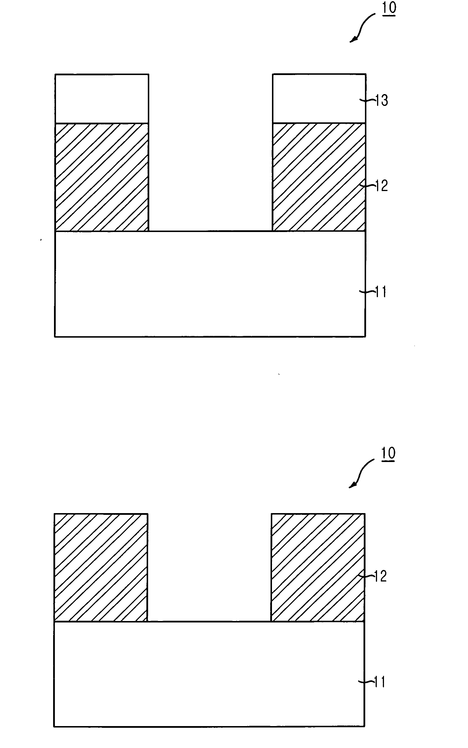
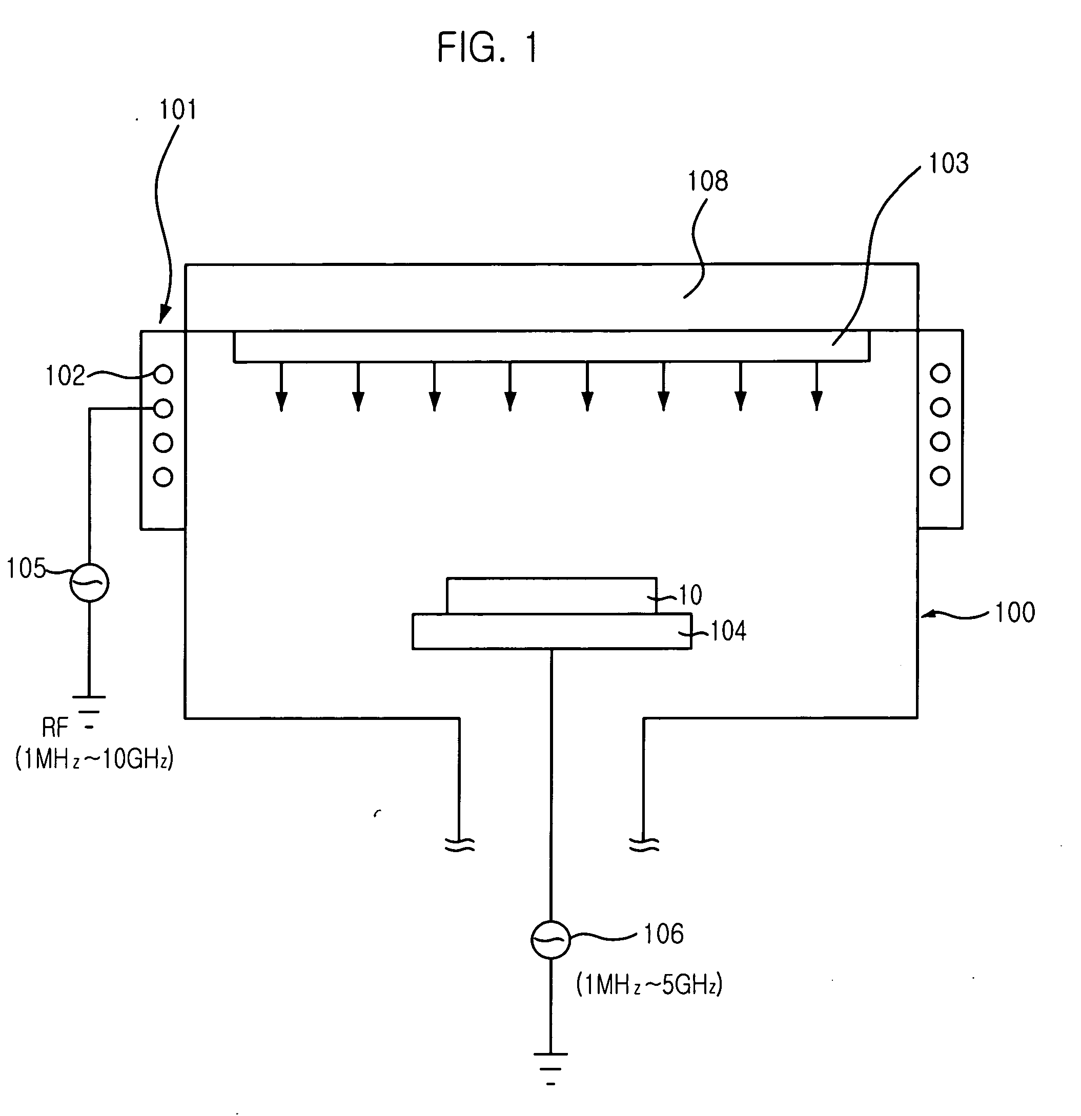
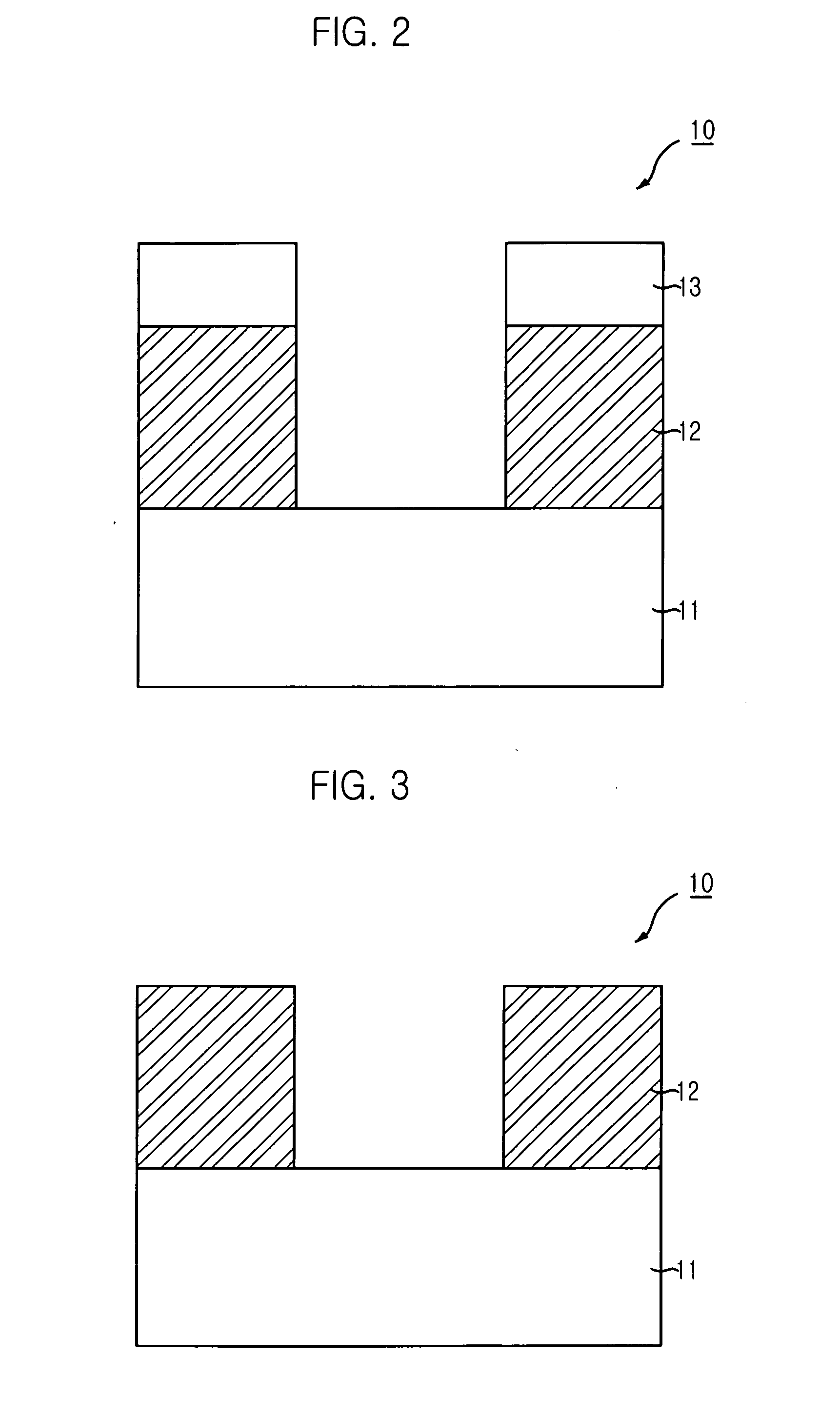
[0029] A method for removing a photoresist pattern in accordance with the present invention is carried out by employing a high density plasma (HDP) dry etching process. The HDP dry etching process executes the etching by using ionized gaseous particles. In more detail of this HDP dry etching process, an etch source gas is provided to a chamber and then, a layer adsorbed onto a surface of a wafer is removed by controlling those ionized gaseous particles and radicals produced by applying a source power and a bias power.

[0030] For realization of the HDP dry etching process, an apparatus for the HDP with a density of at least approximately 5×10⁸ / cm3 to approximately 5×10¹³ / cm3 is used. The HDP apparatus includes an electron cyclotron resonance (ECR) plasma reactor, a helicon plasma reactor using a helical or whistler wave, a helical resonator plasma reactor, and an inductively coupled plasma (ICP) reactor. A decoupled plasma source (DPS) reactor and a transformer coupled plasma (TCP) re...

second embodiment

[0048] Hereinafter, the present invention in regards of a method for forming a metal line by employing the above described photoresist removal method will be described in detail with reference to FIGS. 13A to 13G.

[0049] Referring to FIG. 13A, a substrate 20 precedently cleaned by a cleaning process is provided. The cleaning process can be carried out by using a solution of diluted hydrofluoric (HF) acid and subsequently a mixture solution of ammonium hydroxide (NH4OH), H2O2 and H2O, which is called SC-1 solution, or first using buffered oxide etchant (BOE) and then the SC-1 solution.

[0050] Next, although not illustrated, a well ion implantation process and a threshold ion implantation process are carried out to form a well region and a threshold ion implantation region. At this time, a screen oxide layer can be formed on the substrate 20 before the performance of the well ion implantation process and the threshold ion implantation process in order to prevent the substrate 20 from b...


PUM

PropertyMeasurementUnit
Temperatureaaaaaaaaaa
Poweraaaaaaaaaa

Abstract

Disclosed are a method for removing a photoresist layer and a method for forming a metal line using the same. The method for removing a photoresist pattern, including the steps of: forming a bottom layer on a substrate by using the photoresist pattern as a mask; and removing the photoresist pattern with use of a high density plasma (HDP) apparatus. The method for forming a metal line, including the steps of: preparing a semi-finished substrate including an inter-layer insulation layer; forming a photoresist pattern on the inter-layer insulation layer; forming an opening by etching the inter-layer insulation layer with use of the photoresist pattern as an etch mask; removing the photoresist pattern by using a high density plasma (HDP) apparatus; and forming the metal line by filling the opening with a predetermined material.

Description

FIELD OF THE INVENTION [0001] The present invention relates to a method for removing a photoresist layer and a method for forming a metal line in a semiconductor device using the same; and, more particularly, to a method for removing a photoresist layer in a semiconductor device including a low-k dielectric layer etched by using the photoresist layer and a method for forming a metal line in a semiconductor device using the same. DESCRIPTION OF RELATED ARTS [0002] In semiconductor device fabrication processes, a patterning process, which is one essential fabrication process, adopts a wet etching process or a dry etching process using a photoresist pattern of which main component is carbon as an etch mask. After the etching process, the photoresist pattern is removed by a strip process. Generally, the strip process is carried out by using a solution containing hydrogen peroxide (H2O2), sulfuric acid (H2SO4) or the like, or a gas such as oxygen (O2), nitrogen (N2), hydrogen (H2) or the...

Claims


Application Information

Patent Timeline
IPC IPC(8): H01L21/302H01L21/461
CPCG03F7/427H01L21/02063H01L21/0274H01L21/31138H01L21/76802H01L21/28
Inventor RYU, SANG-WOOK
Owner KEY FOUNDRY CO LTD
Why Eureka
Try Eureka