Tunable microwave devices with auto-adjusting matching circuit

a matching circuit and microwave technology, applied in the field of tunable microwave devices with auto-adjusting matching circuits, can solve the problems of not meeting the requirements of large data transmission of the future, the speed and quality of gsm will not meet the requirements of wireless applications, and the 50 ohm design target is never perfectly m

Active Publication Date: 2006-07-20
NXP USA INC
View PDF98 Cites 198 Cited by
  • Summary
  • Abstract
  • Description
  • Claims
  • Application Information

AI Technical Summary

Benefits of technology

[0034] In yet another embodiment of the present invention is provided an auto-adjusting matching circuit, comprising a first and second coupler to sample an incoming signal and an outgoing signal, a matching network to receive the incoming signal and including a plurality of matching network elements comprising voltage tunable dielectric capacitors, wherein the matching network is capable of automatically adjusting an impedance of the incoming signal, and a power control & logic unit to produce a voltage to output ports from a High Voltage Application Specific Integrated Circuit to the plurality of matching network elements.

Problems solved by technology

However, supporting these applications using wireless techniques poses a significant technical challenge.
However, the speed and quality of GSM will not meet the requirements of the large data transmission of the future.
However, this 50 ohm design target is never perfectly met and also an antenna's impedance is never consistently 50 ohms over all conditions and frequencies of operation.
Given the reciprocal nature of most radios with antennas, this mismatch reduces the amount of power received by the radio from the antenna during reception.
Because the mobile phone is operated in various environments, the antenna is “detuned”, resulting in impedance at its I / O port which can vary wildly.
Regardless of why the two impedances may not be matched, the greater the difference, the greater the power level reflected and the lower the power transferred (transmitted or received), thus lowering the overall efficiency of the RF system (antenna+radio).
Also, antennas often compromise bandwidth in exchange for greater gain (efficiency) or reduced size.
This results in greater variation of its impedance over the frequency of operation.
A perfect impedance match corresponds to a VSWR 1:1, but in practice it will never be achieved.
With a fixed matching network, an amplifier which had been tuned for peak efficiency at the maximum output power level will show severely degraded efficiency as the gain is lowered and the output power drops.
This limits the efficient operating range of an amplifier to a narrow range of frequencies and a small range of power and bias settings.
Digital implementations of impedance matching networks are problematic due to the delays through the digital processors.
These delays cause a phase difference between the incident and synthesized signals which results in an amplitude difference that worsens the return loss.
This problem is generally alleviated by using a faster, but more costly and higher power consuming digital converter and processor.
A problem with the above method is that adaptations of the antenna matching network may be effected in response to reductions in signal strength, when said reductions occur due to reasons other than antenna mismatch; for example, when the variations are due to mismatch in several mobile standards such as switching from GSM mode to EDGE mode.
Therefore, adaptations do not improve transmission characteristics and at worst may make the transmission characteristics worse.
Output matching networks consisting of lumped capacitors (standard ceramic or tantalum capacitors), varactors, inductors, transmission lines, or transformers, suffer because the loss associated with the individual components.
At the RF frequencies the more components used in the network, the aggregate of the individual component loss will worsen the total loss of the matching network.
These devices suffer from a limited qualify factor and tuning range, and exhibit a low voltage swing capability limited by the forward biasing of PN junctions or silicon dioxide breakdown, thus inadequate for high performance RF applications.
However, semiconductor diode varactors suffer from low Q factors (especially at high frequencies), low power handling, and high intermodulation distortion.
Copper-based micromachined tunable capacitors, relying on laterally actuating a dielectric slab between two sets of copper electrodes, have been developed to obtain an improved quality factor but suffer from a small tuning range due to the dielectric layer warpage caused by the film strain gradient.
However, due to the excessive silicon resistive loss, the devices exhibit low quality factors at high frequencies.
However, besides the low quality factor caused by the large silicon resistive loss, complex fluidic packaging is required not suitable for mobile applications.
However, such materials have the undesirable properties of low phase change with voltage which is the main parameter of interest between the conductor line and the ground plane.
Embedded mobile phone antennas have significant performance issues such as dramatic drop in efficiencies when operating conditions change from free space (in a hands-free cradle) to in-situ (against head / hand), with typical efficiencies going from 70% to 25% for the high bands and from 50% dropping down to 10% for the low bands.
Also antenna bandwidths often compromises band-edge performance, especially for antennas having aggressive size reduction, the laws of physics limits gain bandwidth product possible for a given antenna volume.

Method used


Image

  • Tunable microwave devices with auto-adjusting matching circuit
  • Tunable microwave devices with auto-adjusting matching circuit
  • Tunable microwave devices with auto-adjusting matching circuit

Examples


Embodiment Construction

[0049] In the following detailed description, numerous specific details are set forth in order to provide a thorough understanding of the invention. However, it will be understood by those skilled in the art that the present invention may be practiced without these specific details. In other instances, well-known methods, procedures, components and circuits have not been described in detail so as not to obscure the present invention.

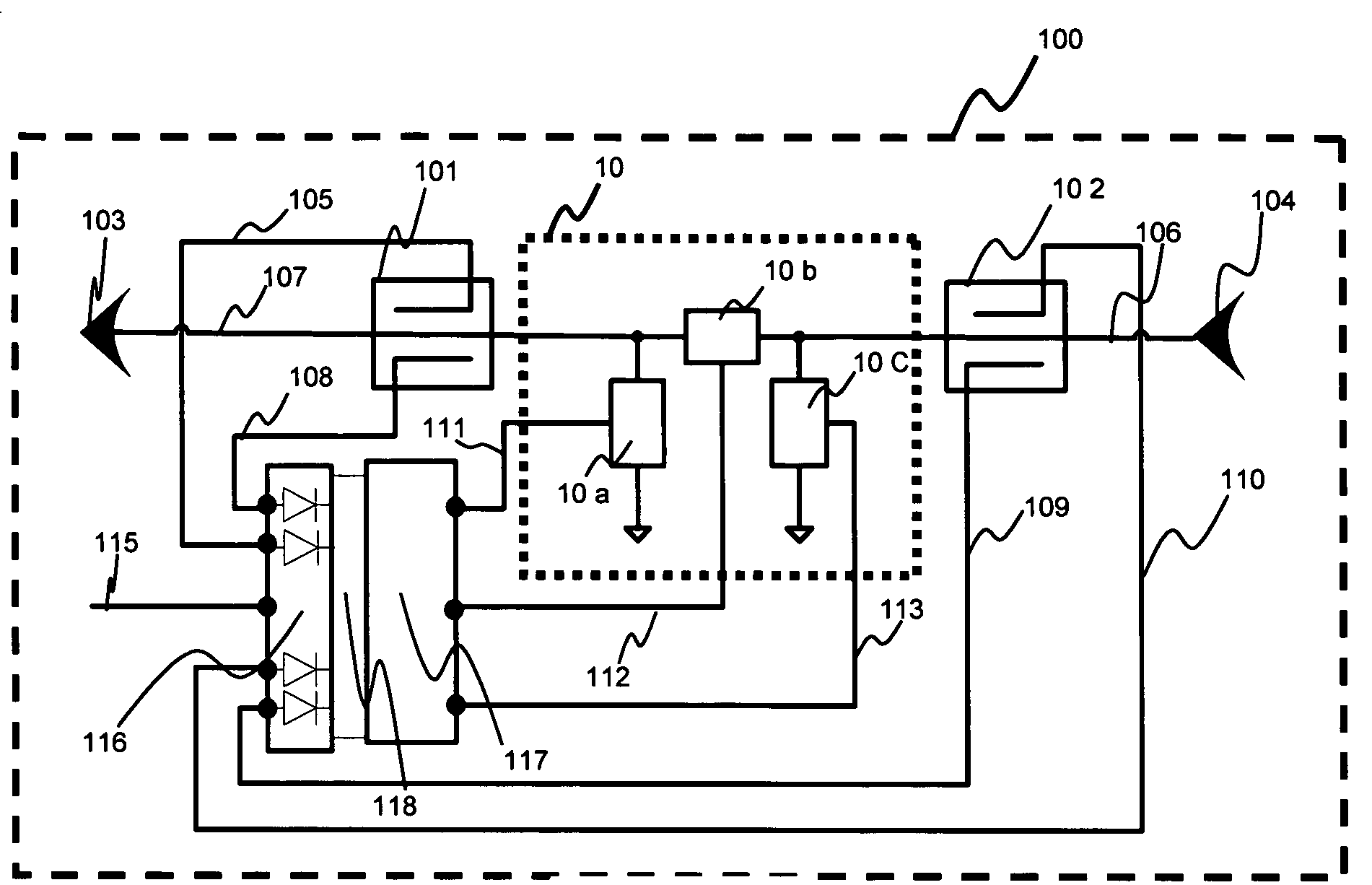
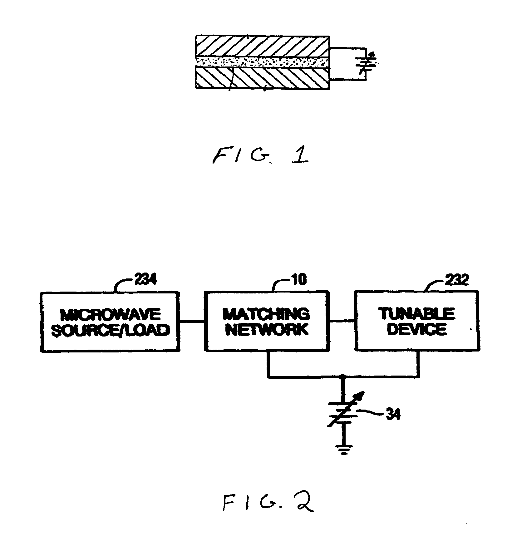
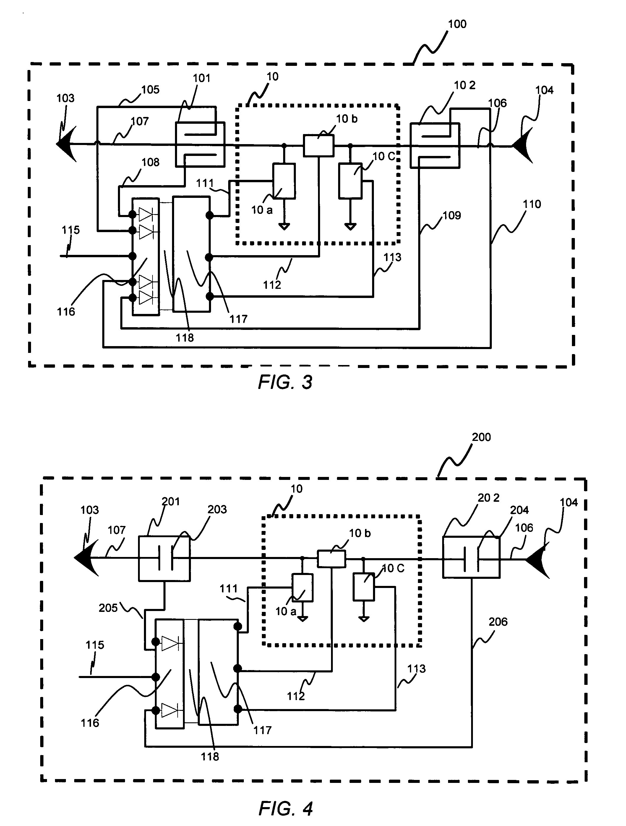
[0050] An impedance matching network or circuit, may be a combination of reactive elements connected between a circuit and at least one load that transform the load impedance into another impedance value to achieve improved performance such as maximum power transfer, reduced reflections, or optimum load performance. An impedance matching network may be made up of a combination of lumped elements, (resistors, capacitors, and inductors), or distributed elements (transmission lines of varying characteristic impedance and length). Similarly, an impedance ma...


PUM


Abstract

An embodiment of the present invention provides an apparatus, comprising an input port and a dynamic impedance matching network capable of determining a mismatch at the input port and dynamically changing the RF match by using at least one matching element that includes at least one voltage tunable dielectric capacitor. The matching network may be a “Pi”, a “T”, or “ladder” type network and the apparatus may further comprise at least one directional coupler capable of signal collection by sampling a portion of an incident signal, a reflected signal or both. In an embodiment of the present invention, the apparatus may also include a control and power control & logic unit (PC LU) to convert input analog signals into digital signals and sensing VSWR phase and magnitude and processing the digital signals using an algorithm to give it a voltage value and wherein the voltage values may be compared to values coming from the coupler and once compared and matched, the values may be passed to a Hi Voltage Application Specific Integrated Circuit (HV ASIC) to transfer and distribute compensatory voltages to the matching network elements.

Description

CROSS REFERENCED TO RELATED APPLICATIONS [0001] This application is a continuation in part of application Ser. No. 10 / 938,898 entitled “TUNABLE MICROWAVE DEVICES WITH AUTO-ADJUSTING MATCHING CIRCUIT” filed 10 Sep. 2004, which was a continuation of application Ser. No. 10 / 455,901 entitled “TUNABLE MICROWAVE DEVICES WITH AUTO-ADJUSTING MATCHING CIRCUIT” filed 6 Jun. 2003 now U.S. Pat. No. 6,864,757, which was a divisional of application Ser. No. 09 / 909,187, now U.S. Pat. No. 6,590,468, entitled “TUNABLE MICROWAVE DEVICES WITH AUTO-ADJUSTING MATCHING CIRCUIT” which claimed the benefit of U.S. provisional application No. 60 / 219,500 filed Jul. 20, 2000. BACKGROUND OF THE INVENTION [0002] Wireless communications is a rapidly growing segment of the communications industry, with the potential to provide high-speed high-quality information exchange between portable devices located anywhere in the world. Potential applications enabled by this technology include, but are not limited to, multim...

Claims


Application Information

Patent Timeline
Patent Type & Authority Applications(United States)
IPC IPC(8): H03F3/04H04B1/04H01Q11/12
CPCH01P5/04H01Q1/242H03F1/56H03F3/60H03H7/40H04B1/0458
Inventor MENDOLIA, GREGMARTIN, JAMES ANDREW IIIKHAYO, IZZDU TOIT, CORNELIS FREDERIKBACHMANN, HEINZMCKINZIE, WILLIAM
Owner NXP USA INC
Why Eureka
Try Eureka